Embed Size (px)
Citation preview
Materials Letters 94 (2013) 86–88
Contents lists available at SciVerse ScienceDirect
Materials Letters
0167-57
http://d
n Corr
E-m
journal homepage: www.elsevier.com/locate/matlet
Black germanium produced by inductively coupled plasma etching
Sandra Schicho, Abdelatif Jaouad n, Christian Sellmer, Denis Morris, Vincent Aimez, Richard Ar�es
Centre de Recherches en Nanofabrication et Nanocaracterisation (CRN2), Institut Interdisciplinaire d’Innovation Technologique (3IT), Universite de Sherbrooke, Sherbrooke, Quebec,
Canada J1K 2R1
a r t i c l e i n f o
Article history:
Received 11 September 2012
Accepted 6 December 2012Available online 20 December 2012
Keywords:
Black Ge
Superhydrophobicity
ICP etching
High-energy photoluminescence
7X/$ - see front matter & 2012 Elsevier B.V.
x.doi.org/10.1016/j.matlet.2012.12.014
esponding author.
ail address: [email protected]
a b s t r a c t
We report on a lithography-free self-organized inductively coupled plasma (ICP) etching process to
manufacture nanostructured Ge surfaces with a strong absorbance in the visible and near-infrared
wavelength region, so-called black germanium. Scanning electron micrographs reveal the presence of
vertical tapered needles, a few tens of mm long and with a mean width of about 500 nm. The samples
show very low reflectance and superhydrophobic characteristics that open up a wide range of electro-
optical and microfluidic applications. Contrary to bulk Ge, black Ge shows a low temperature
photoluminescence emission band at 650 nm, which can be a sign of quantum confinement or of
recombination in GeOx-associated defects. Obtaining black Ge by ICP allows adjusting physical
properties of the layer by controlling the plasma parameters.
& 2012 Elsevier B.V. All rights reserved.
1. Introduction
Black silicon—a needle-like surface modification of crystallinesilicon—was discovered as an initially unwanted side effect of RIEdeep etching of silicon [1]. Today, its high absorbance is used forimage sensors with increased sensitivity and thermal imagingcameras [2]. Furthermore, it is used in high-efficiency photode-tectors [3,4] and terahertz technology [5]. Due to its similarproperties similar applications can be considered for black ger-manium that would allow, e.g., to extend the detection range ofphotodetectors further into the infrared wavelength region.
Conventional multilayer antireflective coatings (ARCs) for, e.g.,solar cells are incident angle- and wavelength-dependent, and astepped refractive index approach is used. Black Ge can potentiallyreplace these complicated ARC stacks since it does not show theselimitations. First silicon solar cells using black Si have already beendemonstrated by NREL [6] and other laboratories [7,8]. Due to the factthat the low reflectance stretches over a wider wavelength region,nanostructured Ge could replace black Si as a more effective ARC.
The superhydrophobicity of black Ge is worth mentioning ,whichmakes it appealing for microfluidic devices where a very low flowresistance is required for minimal energy consumption [9,10], andthe large surface-to-volume ratio, which suggests an application asdurable electrode for, e.g., lithium-ion batteries with prolongedlifetimes [11].
Already in 1978 Gilbert et al. reported on black Ge surfacesthat were developed after etching sputtered non-crystalline Ge
All rights reserved.
(A. Jaouad).
films in H2O2 [12]. Chueh et al. achieved nanoneedle-like, blackappearing Ge surfaces by using a Ni-catalyzed vapor depositionprocess [13]. With both methods the nanoneedle structure is hardto control. With laser etching under SF6 atmosphere, conicalmicrostructures with nanospikes on top were achieved by Nayaket al. Varying laser fluence and number of shots provides thepotential to change the appearance, density or regularity of thefeatures [14].
We present an ICP process to achieve black germanium with ahigh reproducibility. Two power supply sources (coil and platen)regulate the chemical etching by neutrals and radicals andphysical etching by ions separately. Hence, a good control overthe etched structure can be realized.
2. Experimental
Small pieces of p-doped germanium were etched using amultiplex advanced silicon etcher (Surface Technology Systems).The used etching process is derived from the so-called Bosch-Process for deep, anisotropic etching of Si and is based on thealternation of several etching and passivation cycles [15]. Theparameters to achieve black Ge are summarized in Table 1.
To evaluate the hydrophobicity, contact angle measurementswere carried out by disposing a droplet of either water or methanolonto the Ge surface. A high resolution image was taken and thecontact angle was determined by a software. Photoluminescencewas measured at room temperature using a commercial PhilipsPLM-150 mapper. A Nd:YAG laser emitting at 1064 nm served asexcitation source while the luminescence was detected by anInGaAs photodiode array. Additional temperature-dependent PL
S. Schicho et al. / Materials Letters 94 (2013) 86–88 87
measurements at 650 nm were carried out using a green diodelaser (l¼532 nm) as excitation source. The laser power was kept at15 mW and a liquid nitrogen cooled Ge detector recorded the PLemission with lock-in technique.
3. Results and discussion
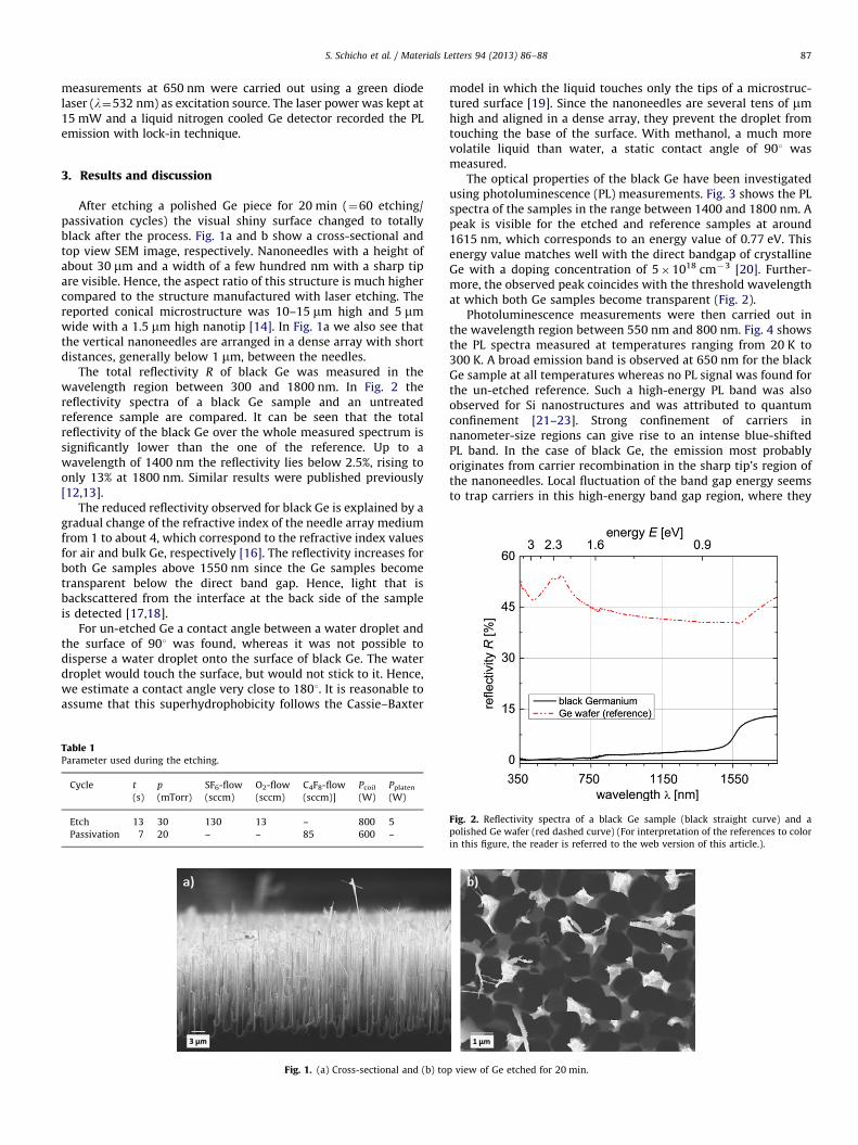
After etching a polished Ge piece for 20 min (¼60 etching/passivation cycles) the visual shiny surface changed to totallyblack after the process. Fig. 1a and b show a cross-sectional andtop view SEM image, respectively. Nanoneedles with a height ofabout 30 mm and a width of a few hundred nm with a sharp tipare visible. Hence, the aspect ratio of this structure is much highercompared to the structure manufactured with laser etching. Thereported conical microstructure was 10–15 mm high and 5 mmwide with a 1.5 mm high nanotip [14]. In Fig. 1a we also see thatthe vertical nanoneedles are arranged in a dense array with shortdistances, generally below 1 mm, between the needles.
The total reflectivity R of black Ge was measured in thewavelength region between 300 and 1800 nm. In Fig. 2 thereflectivity spectra of a black Ge sample and an untreatedreference sample are compared. It can be seen that the totalreflectivity of the black Ge over the whole measured spectrum issignificantly lower than the one of the reference. Up to awavelength of 1400 nm the reflectivity lies below 2.5%, rising toonly 13% at 1800 nm. Similar results were published previously[12,13].
The reduced reflectivity observed for black Ge is explained by agradual change of the refractive index of the needle array mediumfrom 1 to about 4, which correspond to the refractive index valuesfor air and bulk Ge, respectively [16]. The reflectivity increases forboth Ge samples above 1550 nm since the Ge samples becometransparent below the direct band gap. Hence, light that isbackscattered from the interface at the back side of the sampleis detected [17,18].
For un-etched Ge a contact angle between a water droplet andthe surface of 901 was found, whereas it was not possible todisperse a water droplet onto the surface of black Ge. The waterdroplet would touch the surface, but would not stick to it. Hence,we estimate a contact angle very close to 1801. It is reasonable toassume that this superhydrophobicity follows the Cassie–Baxter
Table 1Parameter used during the etching.
Cycle t p SF6-flow O2-flow C4F8-flow Pcoil Pplaten
(s) (mTorr) (sccm) (sccm) (sccm)] (W) (W)
Etch 13 30 130 13 – 800 5
Passivation 7 20 – – 85 600 –
Fig. 1. (a) Cross-sectional and (b) to
model in which the liquid touches only the tips of a microstruc-tured surface [19]. Since the nanoneedles are several tens of mmhigh and aligned in a dense array, they prevent the droplet fromtouching the base of the surface. With methanol, a much morevolatile liquid than water, a static contact angle of 901 wasmeasured.
The optical properties of the black Ge have been investigatedusing photoluminescence (PL) measurements. Fig. 3 shows the PLspectra of the samples in the range between 1400 and 1800 nm. Apeak is visible for the etched and reference samples at around1615 nm, which corresponds to an energy value of 0.77 eV. Thisenergy value matches well with the direct bandgap of crystallineGe with a doping concentration of 5�1018 cm�3 [20]. Further-more, the observed peak coincides with the threshold wavelengthat which both Ge samples become transparent (Fig. 2).
Photoluminescence measurements were then carried out inthe wavelength region between 550 nm and 800 nm. Fig. 4 showsthe PL spectra measured at temperatures ranging from 20 K to300 K. A broad emission band is observed at 650 nm for the blackGe sample at all temperatures whereas no PL signal was found forthe un-etched reference. Such a high-energy PL band was alsoobserved for Si nanostructures and was attributed to quantumconfinement [21–23]. Strong confinement of carriers innanometer-size regions can give rise to an intense blue-shiftedPL band. In the case of black Ge, the emission most probablyoriginates from carrier recombination in the sharp tip’s region ofthe nanoneedles. Local fluctuation of the band gap energy seemsto trap carriers in this high-energy band gap region, where they
p view of Ge etched for 20 min.
Fig. 2. Reflectivity spectra of a black Ge sample (black straight curve) and a
polished Ge wafer (red dashed curve) (For interpretation of the references to color
in this figure, the reader is referred to the web version of this article.).
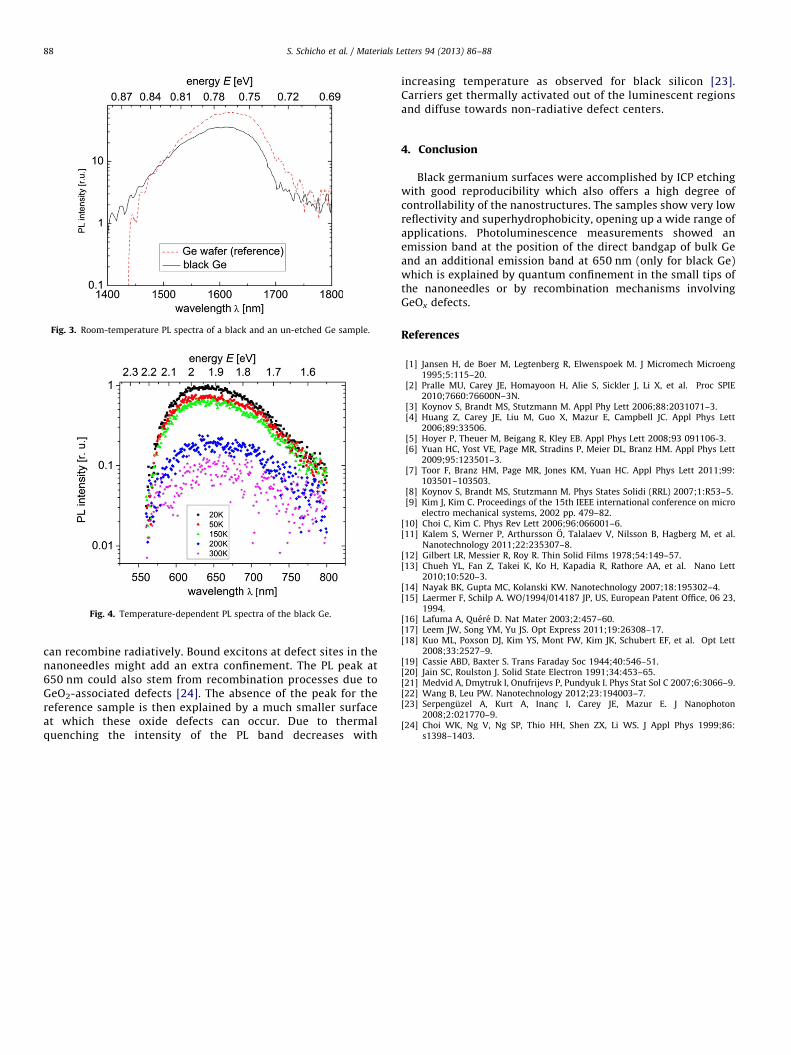
Fig. 3. Room-temperature PL spectra of a black and an un-etched Ge sample.
Fig. 4. Temperature-dependent PL spectra of the black Ge.
S. Schicho et al. / Materials Letters 94 (2013) 86–8888
can recombine radiatively. Bound excitons at defect sites in thenanoneedles might add an extra confinement. The PL peak at650 nm could also stem from recombination processes due toGeO2-associated defects [24]. The absence of the peak for thereference sample is then explained by a much smaller surfaceat which these oxide defects can occur. Due to thermalquenching the intensity of the PL band decreases with
increasing temperature as observed for black silicon [23].Carriers get thermally activated out of the luminescent regionsand diffuse towards non-radiative defect centers.
4. Conclusion
Black germanium surfaces were accomplished by ICP etchingwith good reproducibility which also offers a high degree ofcontrollability of the nanostructures. The samples show very lowreflectivity and superhydrophobicity, opening up a wide range ofapplications. Photoluminescence measurements showed anemission band at the position of the direct bandgap of bulk Geand an additional emission band at 650 nm (only for black Ge)which is explained by quantum confinement in the small tips ofthe nanoneedles or by recombination mechanisms involvingGeOx defects.
References
[1] Jansen H, de Boer M, Legtenberg R, Elwenspoek M. J Micromech Microeng1995;5:115–20.
[2] Pralle MU, Carey JE, Homayoon H, Alie S, Sickler J, Li X, et al. Proc SPIE2010;7660:76600N–3N.
[3] Koynov S, Brandt MS, Stutzmann M. Appl Phy Lett 2006;88:2031071–3.[4] Huang Z, Carey JE, Liu M, Guo X, Mazur E, Campbell JC. Appl Phys Lett
2006;89:33506.[5] Hoyer P, Theuer M, Beigang R, Kley EB. Appl Phys Lett 2008;93 091106-3.[6] Yuan HC, Yost VE, Page MR, Stradins P, Meier DL, Branz HM. Appl Phys Lett
2009;95:123501–3.[7] Toor F, Branz HM, Page MR, Jones KM, Yuan HC. Appl Phys Lett 2011;99:
103501–103503.[8] Koynov S, Brandt MS, Stutzmann M. Phys States Solidi (RRL) 2007;1:R53–5.[9] Kim J, Kim C. Proceedings of the 15th IEEE international conference on micro
electro mechanical systems, 2002 pp. 479–82.[10] Choi C, Kim C. Phys Rev Lett 2006;96:066001–6.[11] Kalem S, Werner P, Arthursson O, Talalaev V, Nilsson B, Hagberg M, et al.
Nanotechnology 2011;22:235307–8.[12] Gilbert LR, Messier R, Roy R. Thin Solid Films 1978;54:149–57.[13] Chueh YL, Fan Z, Takei K, Ko H, Kapadia R, Rathore AA, et al. Nano Lett
2010;10:520–3.[14] Nayak BK, Gupta MC, Kolanski KW. Nanotechnology 2007;18:195302–4.[15] Laermer F, Schilp A. WO/1994/014187 JP, US, European Patent Office, 06 23,
1994.[16] Lafuma A, Quere D. Nat Mater 2003;2:457–60.[17] Leem JW, Song YM, Yu JS. Opt Express 2011;19:26308–17.[18] Kuo ML, Poxson DJ, Kim YS, Mont FW, Kim JK, Schubert EF, et al. Opt Lett
2008;33:2527–9.[19] Cassie ABD, Baxter S. Trans Faraday Soc 1944;40:546–51.[20] Jain SC, Roulston J. Solid State Electron 1991;34:453–65.[21] Medvid A, Dmytruk I, Onufrijevs P, Pundyuk I. Phys Stat Sol C 2007;6:3066–9.[22] Wang B, Leu PW. Nanotechnology 2012;23:194003–7.[23] Serpenguzel A, Kurt A, Inanc- I, Carey JE, Mazur E. J Nanophoton
2008;2:021770–9.[24] Choi WK, Ng V, Ng SP, Thio HH, Shen ZX, Li WS. J Appl Phys 1999;86:
s1398–1403.