Embed Size (px)
Citation preview
Materials Chemistry and Physics 83 (2004) 43–47
Cathodoluminescence properties of undoped and Al-doped ZnO thinfilms deposited on glass substrate by spray pyrolysis
A. El Hichoub,c,∗, M. Addoua,∗, A. Bougrinea, R. Douniaa,J. Ebothéb, M. Troyonb, M. Amrania
a Lab. d’Optoélectronique et de Physico-Chimie des Matériaux, Faculté des Sciences, Université Ibn Tofail, B.P. 133, Kénitra, Moroccob UFR Sciences, Université de Reims, UTAP-LMET, UPRES EA 2061, 21 rue Clément Ader, 51685 Reims Cedex 2, France
c Faculté des Sciences et Techniques Guéliz, Université Cadi Ayyad, G.E.M.O. B.P. 549, Marrakech, Morocco
Received 21 March 2003; received in revised form 8 May 2003; accepted 8 August 2003
Abstract
Undoped and Al-doped zinc oxide (ZnO) thin films have been prepared by spray pyrolysis (SP), and the effect of doping on structuralproperties and cathodoluminescence (CL) imaging and spectroscopy has been investigated. These films, deposited at an optimal substratetemperature (Ts = 450◦C), have a hexagonal close-packed structure. At room temperature, the CL spectra of the undoped and doped ZnOfilms exhibit the common near ultra-violet band gap peak atλ = 382 nm, but they differ as regard to the visible emissions. The undopedZnO emits an intensive blue-green light atλ = 520 nm and a red emission atλ = 672 nm. The presence of aluminium gives rise to a newlight typical of the intrinsic behaviour of the material. CL imaging of the undoped ZnO films shows that the luminescence is located atdefined sites with a grain-like structure inherent to the sample surface morphology. The presence of aluminium leads to a homogenousrepartition of the emitting centres.© 2003 Elsevier B.V. All rights reserved.
Keywords: ZnO; Al; Spray pyrolysis; Cathodoluminescence; Transparent conducting films
1. Introduction
Transparent conducting zinc oxide (ZnO) has recentlygained much attention due to the many advantages over otheroxide thin films such as In2O3, CdSnO4 or SnO2. These ad-vantages include non-toxicity, good electrical, optical andpiezoelectric behaviours, stability in hydrogen plasma at-mosphere and low price[1–3]. Moreover, ZnO thin filmshave potential applications, such as gas sensors devices[4],transparent electrodes[3] and piezoelectric devices[5]. ZnOcan be doped with a wide variety of ions to meet the de-mands of several application fields. Typical dopants thathave been used to produce conducting ZnO films belong tothe group IIIa elements of the periodic table (Al, In, Ga,etc.). There are several deposition techniques which havebeen employed to grow doped ZnO and undoped ZnO thinfilms, including chemical vapour deposition (CVD)[6,7],magnetron sputtering[8,9], pulsed laser deposition (PLD)
∗ Corresponding authors. Tel.:+212-61355725; fax:+212-37376931.E-mail addresses: [email protected] (A. El Hichou), [email protected] (M. Addou).
[10,11] and spray pyrolysis (SP)[12–15]. In comparison ofthe films grown by SP, it is quite simple and the requiredset-up is less expansive and flexible for process modifica-tions. Due to the use of less expansive chemicals at ambientpressure conditions, it is attractive from an economical pointof view also. Additionally, by using this technique one canproduce large area films without the need of an ultra highvacuum and the produced films can be controlled step bystep.
Whereas many works dealing with the physical proper-ties of the intrinsic and Al-doped ZnO films obtained by SPhave been published[15–17], the investigation of their lu-minescence characteristics remains very limited, especially,the cathodoluminescence (CL).
In this work, we report the effect of doping with alu-minium on the structural and CL properties. The CL anal-ysis used together with the scanning electron microscopyimaging, presents the advantage of the high-resolution char-acterisation. Indeed, this method provides images of thedefect distributions, which are interesting for the evaluationof the material purity. A local investigation as done herebyis justified by the increasing trend of miniaturising devices.
0254-0584/$ – see front matter © 2003 Elsevier B.V. All rights reserved.doi:10.1016/j.matchemphys.2003.08.015
44 A. El Hichou et al. / Materials Chemistry and Physics 83 (2004) 43–47
2. Experimental
The SP operating set and the details on the procedure ap-plied for the deposition of the investigated ZnO films havebeen described elsewhere[18]. It can be briefly remindedthat the spraying bath consisted of a 0.05 M solution ofFLUKA ZnCl2 product. A 5% of Al2(SO4)3 was made forthe Al-doped ZnO films. This bath was always buffered by asmall amount of hydrochloric acid. The nozzle was directedtowards a substrate with a spraying flow rate of 5 ml min−1.This substrate was made of bare glass sheets whose temper-ature was maintained constant atTs = 450◦C, that is knownto be the optimum condition for this material formation. Thesame film thickness of 0.3�m estimated from the depositiontime was retained. A good agreement was obtained withthe value deduced from the cross-sectional images usingtransmission electron microscopy. The compositional anal-ysis of the films as performed with an EDAX 9100 analyserindicated that the 5% aluminium percentage of the spray-ing bath is quite recovered in the Al-doped ZnO samples.The structural aspect was investigated by X-ray diffractionusing Cu K� radiation. The CL set used was a home-madesystem that we have developed to perform near-field CLmicroscopy[19]. This one is based on the combination ofa scanning force microscope (SFM) and a field emissionscanning electron microscope (FESEM GEMINI 982 fromLEO), the mechanical details of which are reported in[19].Since the CL intensity in the near-field regime was underthe minimum acceptable level of signal to noise ratio tominimise the noise of the images[20], we have preferred tocollect the photons in the far-field mode with a multimodeoptical fibre(NA = 0.48) placed close to the sample sur-face (≈50�m). The CL images were acquired with a fixedelectron beam at low accelerating voltage (4 kV), the samplebeing scanned under the fibre thanks to the scanning piezotube. Our CL system, in association with a spectrometer(Triax 190 from JOBIN YVON), allows monochromaticCL imaging as well as acquisition of CL spectra on verylocalised spots of the sample. The spectrometer has a spec-tral resolution of 0.5 nm and is equipped with an N2-cooledCCD detector. Monochromatic CL images can be obtainedby selecting a defined wavelength and by sending the lightto a photomultiplier (PM, R4220P from Hamamatsu). Thesignal is then amplified with an electrometer and imagesof 256× 256 pixels at a line frequency of about 0.1 Hz aregenerated. Panchromatic images are also obtained by direct-ing the light towards the PM without passing through thespectrometer.
3. Results and discussion
3.1. Structural and morphological properties
We employed the X-ray diffraction technique to get a firstimpression of the main crystalline phases and the possible
20 30 40 50 60
Inte
nsit
y (a
.u)
2θ(deg)
(002)
(a )
(b)
(002)
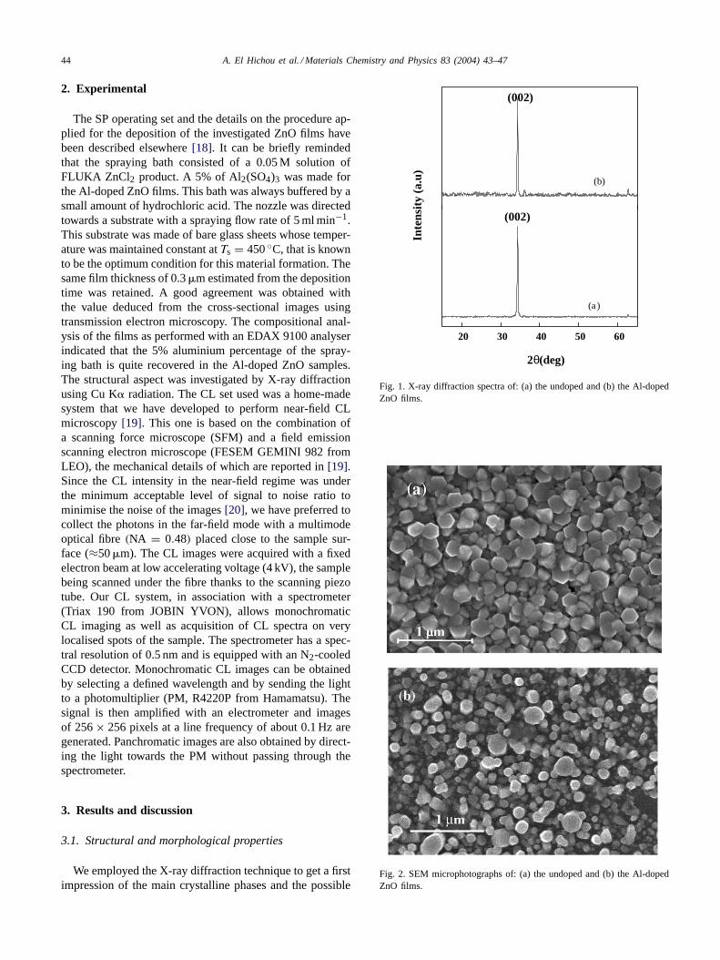
Fig. 1. X-ray diffraction spectra of: (a) the undoped and (b) the Al-dopedZnO films.
Fig. 2. SEM microphotographs of: (a) the undoped and (b) the Al-dopedZnO films.
A. El Hichou et al. / Materials Chemistry and Physics 83 (2004) 43–47 45
400 500 600 700
1000
2000
3000
4000
CL
Int
ensi
ty (
coun
ts)
Wavelength (nm)
300 400 500 600 700 800
2000
4000
6000
8000
10000
12000
CL
Int
ensi
ty (
coun
ts)
Wavelength (nm)
(a)
(b)
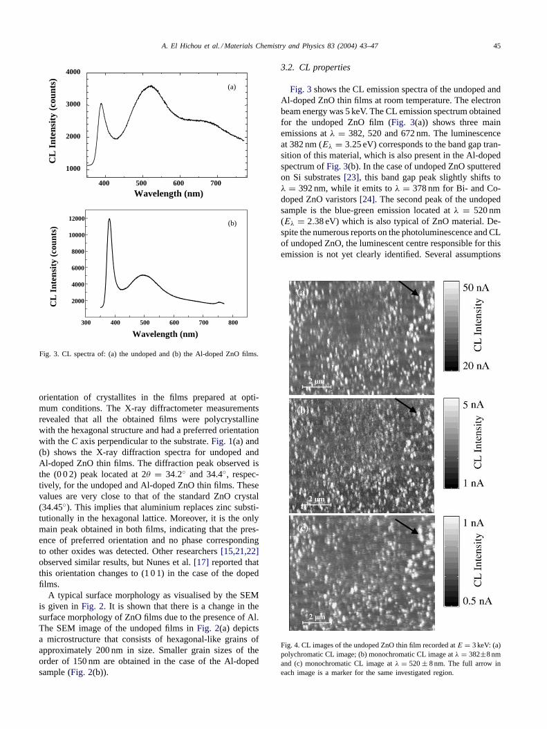
Fig. 3. CL spectra of: (a) the undoped and (b) the Al-doped ZnO films.
orientation of crystallites in the films prepared at opti-mum conditions. The X-ray diffractometer measurementsrevealed that all the obtained films were polycrystallinewith the hexagonal structure and had a preferred orientationwith theC axis perpendicular to the substrate.Fig. 1(a) and(b) shows the X-ray diffraction spectra for undoped andAl-doped ZnO thin films. The diffraction peak observed isthe (0 0 2) peak located at 2θ = 34.2◦ and 34.4◦, respec-tively, for the undoped and Al-doped ZnO thin films. Thesevalues are very close to that of the standard ZnO crystal(34.45◦). This implies that aluminium replaces zinc substi-tutionally in the hexagonal lattice. Moreover, it is the onlymain peak obtained in both films, indicating that the pres-ence of preferred orientation and no phase correspondingto other oxides was detected. Other researchers[15,21,22]observed similar results, but Nunes et al.[17] reported thatthis orientation changes to (1 0 1) in the case of the dopedfilms.
A typical surface morphology as visualised by the SEMis given inFig. 2. It is shown that there is a change in thesurface morphology of ZnO films due to the presence of Al.The SEM image of the undoped films inFig. 2(a) depictsa microstructure that consists of hexagonal-like grains ofapproximately 200 nm in size. Smaller grain sizes of theorder of 150 nm are obtained in the case of the Al-dopedsample (Fig. 2(b)).
3.2. CL properties
Fig. 3shows the CL emission spectra of the undoped andAl-doped ZnO thin films at room temperature. The electronbeam energy was 5 keV. The CL emission spectrum obtainedfor the undoped ZnO film (Fig. 3(a)) shows three mainemissions atλ = 382, 520 and 672 nm. The luminescenceat 382 nm (Eλ = 3.25 eV) corresponds to the band gap tran-sition of this material, which is also present in the Al-dopedspectrum ofFig. 3(b). In the case of undoped ZnO sputteredon Si substrates[23], this band gap peak slightly shifts toλ = 392 nm, while it emits toλ = 378 nm for Bi- and Co-doped ZnO varistors[24]. The second peak of the undopedsample is the blue-green emission located atλ = 520 nm(Eλ = 2.38 eV) which is also typical of ZnO material. De-spite the numerous reports on the photoluminescence and CLof undoped ZnO, the luminescent centre responsible for thisemission is not yet clearly identified. Several assumptions
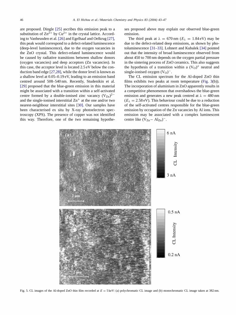
Fig. 4. CL images of the undoped ZnO thin film recorded atE = 3 keV: (a)polychromatic CL image; (b) monochromatic CL image atλ = 382±8 nmand (c) monochromatic CL image atλ = 520± 8 nm. The full arrow ineach image is a marker for the same investigated region.
46 A. El Hichou et al. / Materials Chemistry and Physics 83 (2004) 43–47
are proposed. Dingle[25] ascribes this emission peak to asubstitution of Zn2+ by Cu2+ in the crystal lattice. Accord-ing to Vanheusden et al.[26] and Egelhaaf and Oelkrug[27],this peak would correspond to a defect-related luminescence(deep-level luminescence), due to the oxygen vacancies inthe ZnO crystal. This defect-related luminescence wouldbe caused by radiative transitions between shallow donors(oxygen vacancies) and deep acceptors (Zn vacancies). Inthis case, the acceptor level is located 2.5 eV below the con-duction band edge[27,28], while the donor level is known asa shallow level at 0.05–0.19 eV, leading to an emission bandcentred around 508–540 nm. Recently, Studenikin et al.[29] proposed that the blue-green emission in this materialmight be associated with a transition within a self-activatedcentre formed by a double-ionised zinc vacancy (VZn)2−and the single-ionised interstitial Zn+ at the one and/or twonearest-neighbour interstitial sites[30]. Our samples havebeen characterised ex situ by X-ray photoelectron spec-troscopy (XPS). The presence of copper was not identifiedthis way. Therefore, one of the two remaining hypothe-
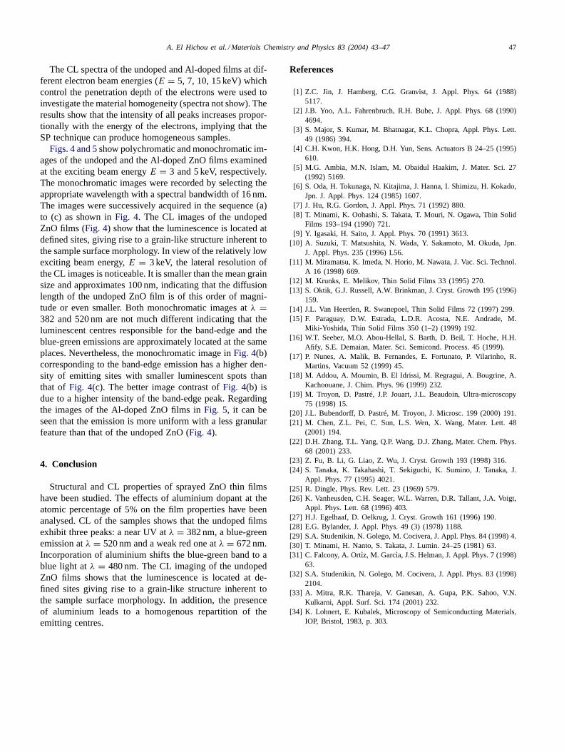
Fig. 5. CL images of the Al-doped ZnO thin film recorded atE = 5 keV: (a) polychromatic CL image and (b) monochromatic CL image taken at 382 nm.
ses proposed above may explain our observed blue-greenemission.
The third peak atλ = 670 nm (Eλ = 1.84 eV) may bedue to the defect-related deep emissions, as shown by pho-toluminescence[31–33]. Lohnert and Kubalek[34] pointedout that the intensity of broad luminescence observed fromabout 450 to 700 nm depends on the oxygen partial pressurein the sintering process of ZnO ceramics. This also suggeststhe hypothesis of a transition within a (VO)x neutral andsingle-ionised oxygen (VO)−.
The CL emission spectrum for the Al-doped ZnO thinfilms exhibits two peaks at room temperature (Fig. 3(b)).The incorporation of aluminium in ZnO apparently results ina competitive phenomenon that overshadows the blue-greenemission and generates a new peak centred atλ = 480 nm(Eλ = 2.58 eV). This behaviour could be due to a reductionof the self-activated centres responsible for the blue-greenemission by occupation of the Zn vacancies by Al ions. Thisemission may be associated with a complex luminescentcentre like (VZn− AlZn)−.
A. El Hichou et al. / Materials Chemistry and Physics 83 (2004) 43–47 47
The CL spectra of the undoped and Al-doped films at dif-ferent electron beam energies (E = 5, 7, 10, 15 keV) whichcontrol the penetration depth of the electrons were used toinvestigate the material homogeneity (spectra not show). Theresults show that the intensity of all peaks increases propor-tionally with the energy of the electrons, implying that theSP technique can produce homogeneous samples.
Figs. 4 and 5show polychromatic and monochromatic im-ages of the undoped and the Al-doped ZnO films examinedat the exciting beam energyE = 3 and 5 keV, respectively.The monochromatic images were recorded by selecting theappropriate wavelength with a spectral bandwidth of 16 nm.The images were successively acquired in the sequence (a)to (c) as shown inFig. 4. The CL images of the undopedZnO films (Fig. 4) show that the luminescence is located atdefined sites, giving rise to a grain-like structure inherent tothe sample surface morphology. In view of the relatively lowexciting beam energy,E = 3 keV, the lateral resolution ofthe CL images is noticeable. It is smaller than the mean grainsize and approximates 100 nm, indicating that the diffusionlength of the undoped ZnO film is of this order of magni-tude or even smaller. Both monochromatic images atλ =382 and 520 nm are not much different indicating that theluminescent centres responsible for the band-edge and theblue-green emissions are approximately located at the sameplaces. Nevertheless, the monochromatic image inFig. 4(b)corresponding to the band-edge emission has a higher den-sity of emitting sites with smaller luminescent spots thanthat of Fig. 4(c). The better image contrast ofFig. 4(b) isdue to a higher intensity of the band-edge peak. Regardingthe images of the Al-doped ZnO films inFig. 5, it can beseen that the emission is more uniform with a less granularfeature than that of the undoped ZnO (Fig. 4).
4. Conclusion
Structural and CL properties of sprayed ZnO thin filmshave been studied. The effects of aluminium dopant at theatomic percentage of 5% on the film properties have beenanalysed. CL of the samples shows that the undoped filmsexhibit three peaks: a near UV atλ = 382 nm, a blue-greenemission atλ = 520 nm and a weak red one atλ = 672 nm.Incorporation of aluminium shifts the blue-green band to ablue light atλ = 480 nm. The CL imaging of the undopedZnO films shows that the luminescence is located at de-fined sites giving rise to a grain-like structure inherent tothe sample surface morphology. In addition, the presenceof aluminium leads to a homogenous repartition of theemitting centres.
References
[1] Z.C. Jin, J. Hamberg, C.G. Granvist, J. Appl. Phys. 64 (1988)5117.
[2] J.B. Yoo, A.L. Fahrenbruch, R.H. Bube, J. Appl. Phys. 68 (1990)4694.
[3] S. Major, S. Kumar, M. Bhatnagar, K.L. Chopra, Appl. Phys. Lett.49 (1986) 394.
[4] C.H. Kwon, H.K. Hong, D.H. Yun, Sens. Actuators B 24–25 (1995)610.
[5] M.G. Ambia, M.N. Islam, M. Obaidul Haakim, J. Mater. Sci. 27(1992) 5169.
[6] S. Oda, H. Tokunaga, N. Kitajima, J. Hanna, I. Shimizu, H. Kokado,Jpn. J. Appl. Phys. 124 (1985) 1607.
[7] J. Hu, R.G. Gordon, J. Appl. Phys. 71 (1992) 880.[8] T. Minami, K. Oohashi, S. Takata, T. Mouri, N. Ogawa, Thin Solid
Films 193–194 (1990) 721.[9] Y. Igasaki, H. Saito, J. Appl. Phys. 70 (1991) 3613.
[10] A. Suzuki, T. Matsushita, N. Wada, Y. Sakamoto, M. Okuda, Jpn.J. Appl. Phys. 235 (1996) L56.
[11] M. Miramatsu, K. Imeda, N. Horio, M. Nawata, J. Vac. Sci. Technol.A 16 (1998) 669.
[12] M. Krunks, E. Melikov, Thin Solid Films 33 (1995) 270.[13] S. Oktik, G.J. Russell, A.W. Brinkman, J. Cryst. Growth 195 (1996)
159.[14] J.L. Van Heerden, R. Swanepoel, Thin Solid Films 72 (1997) 299.[15] F. Paraguay, D.W. Estrada, L.D.R. Acosta, N.E. Andrade, M.
Miki-Yoshida, Thin Solid Films 350 (1–2) (1999) 192.[16] W.T. Seeber, M.O. Abou-Hellal, S. Barth, D. Beil, T. Hoche, H.H.
Afify, S.E. Demaian, Mater. Sci. Semicond. Process. 45 (1999).[17] P. Nunes, A. Malik, B. Fernandes, E. Fortunato, P. Vilarinho, R.
Martins, Vacuum 52 (1999) 45.[18] M. Addou, A. Moumin, B. El Idrissi, M. Regragui, A. Bougrine, A.
Kachoouane, J. Chim. Phys. 96 (1999) 232.[19] M. Troyon, D. Pastré, J.P. Jouart, J.L. Beaudoin, Ultra-microscopy
75 (1998) 15.[20] J.L. Bubendorff, D. Pastré, M. Troyon, J. Microsc. 199 (2000) 191.[21] M. Chen, Z.L. Pei, C. Sun, L.S. Wen, X. Wang, Mater. Lett. 48
(2001) 194.[22] D.H. Zhang, T.L. Yang, Q.P. Wang, D.J. Zhang, Mater. Chem. Phys.
68 (2001) 233.[23] Z. Fu, B. Li, G. Liao, Z. Wu, J. Cryst. Growth 193 (1998) 316.[24] S. Tanaka, K. Takahashi, T. Sekiguchi, K. Sumino, J. Tanaka, J.
Appl. Phys. 77 (1995) 4021.[25] R. Dingle, Phys. Rev. Lett. 23 (1969) 579.[26] K. Vanheusden, C.H. Seager, W.L. Warren, D.R. Tallant, J.A. Voigt,
Appl. Phys. Lett. 68 (1996) 403.[27] H.J. Egelhaaf, D. Oelkrug, J. Cryst. Growth 161 (1996) 190.[28] E.G. Bylander, J. Appl. Phys. 49 (3) (1978) 1188.[29] S.A. Studenikin, N. Golego, M. Cocivera, J. Appl. Phys. 84 (1998) 4.[30] T. Minami, H. Nanto, S. Takata, J. Lumin. 24–25 (1981) 63.[31] C. Falcony, A. Ort̀ız, M. Garc̀ıa, J.S. Helman, J. Appl. Phys. 7 (1998)
63.[32] S.A. Studenikin, N. Golego, M. Cocivera, J. Appl. Phys. 83 (1998)
2104.[33] A. Mitra, R.K. Thareja, V. Ganesan, A. Gupa, P.K. Sahoo, V.N.
Kulkarni, Appl. Surf. Sci. 174 (2001) 232.[34] K. Lohnert, E. Kubalek, Microscopy of Semiconducting Materials,
IOP, Bristol, 1983, p. 303.

![Structure and electrical properties of Eu-doped SrBi ceramics 45 09.pdf · M. Afqir et al. /Processing and Applicationof Ceramics 13 [3] (2019)281–286 Figure 6. Temperature dependence](https://img.pdfslide.fr/doc/110x75/5e4c4a685d9d5115175c987a/structure-and-electrical-properties-of-eu-doped-srbi-45-09pdf-m-afqir-et-al.jpg)


![Noise in distributed Raman amplification [6781-40] · amplification over length of several tens of km which is significantly larger than the distribution length of Erbium Doped Fiber](https://img.pdfslide.fr/doc/110x75/5faede2454006b677403579e/noise-in-distributed-raman-amplification-6781-40-amplification-over-length-of.jpg)


![Application of Infrared Spectroscopy and Pyrolysis-Gas ......mass spectral data with the —chromatographic fingerprintfl in identification of auto mobile paints [8]. Some authors](https://img.pdfslide.fr/doc/110x75/612247122fb297747f12029f/application-of-infrared-spectroscopy-and-pyrolysis-gas-mass-spectral-data.jpg)


![Microstructure of laser metal deposited duplex stainless steel ......welding of duplex stainless steel grades [7, 8]. Therefore, the same phenomena are expected to occur when depositing](https://img.pdfslide.fr/doc/110x75/60ad8418cfcf5514db0daf6a/microstructure-of-laser-metal-deposited-duplex-stainless-steel-welding-of.jpg)
![Improved conductivity and capacitance of interdigital ...mai.group.whut.edu.cn/chs/lw/2016/201702/P... · polymer fabrication techniques with pyrolysis or thermal degradation [21–27]](https://img.pdfslide.fr/doc/110x75/5ff7dcadced30417a4176688/improved-conductivity-and-capacitance-of-interdigital-maigroupwhuteducnchslw2016201702p.jpg)