Embed Size (px)
Citation preview
ELSEVIER Applied Surface Science 123/124 (1998) 319-323
applied surface science
Epitaxial growth of Fe on Fe/GaAs(001) reacted layers
C. Lallaizon a, B. L6pine a,*, S. Ababou a, A. Schussler a, A. Qu6merais ", A. Guivarc'h ", G. J~z~quel ", S. D6putier b, R. Gu6rin b
~ Equipe de Physique des SurJaces et des Interfaces, UMR CNRS-Unil:ersit~ No. 6627, Bgtt. 11C, Campus de Beaulieu, 35042 Rennes, France
b Laboratoire de Chimie du Solide et lnolganique Mol~culaire, UMR CNRS-Unit'ersit~ "~ No. 6511, Campus de Beaulieu, 35042 Rennes, France
Abstract
By using in situ techniques (RHEED, XPS and XPD), we show that the UHV annealing treatment of an epitaxial Fe/GaAs(001) structure in the 400-450°C temperature range leads to the formation of an epitaxial reacted layer. Then, we demonstrate that an epitaxial growth of Fe is possible at room temperature on such a reacted layer. As Fe is usually deposited on GaAs in the 150-200°C temperature range, this study reconciles the epitaxial growth of Fe with the interface disruption and intermixing previously observed at the beginning of the deposition. © 1998 Elsevier Science B.V.
Kevwords: Contact metal/semiconductor; Epitaxy; Ternary compound; Fe; GaAs
1. Introduction
The study of magnetic thin films on semiconduc- tor substrates is of great practical interest due to their potential use in novel semiconductor heterostructure devices. The properties of single-crystal films of iron grown by molecular beam epitaxy (MBE) on GaAs(001) and (110) have been extensively studied [1-10]. Epitaxy in the F e / G a A s system has been attributed to the fact that the lattice constant of GaAs is almost double that of bcc Fe (the mismatch is equal to 1.4%). However, investigations of the mag- netization of Fe on GaAs showed that these films exhibited an anomalous decrease in magnetization per Fe atom deposited with decreasing thin-film thickness. Moreover, numerous X-ray photoemission spectroscopy (XPS) results indicated that Fe pro-
Corresponding author. Tel,: +33-2-99286987; fax: +33-2- 99286198; e-mail: bruno.lepine@univ-rennes 1 .ft.
moted Ga and As out-diffusion when deposited onto GaAs surfaces. The simultaneous occurrence of epi- taxy of Fe and surface disruption of GaAs makes the behavior of the F e / G a A s system highly unusual but, up to now, no clear explanation has been proposed to make coherent these two facts.
In many previously published studies [2,5-10], the substrate was maintained at a temperature in the 150-200°C range during the Fe growth; this was reported by Prinz et al. [2,5,6] as the proper way to obtain epitaxial films of good quality [8-10]. Re- cently, Filipe et al. [8-10] studied the dependence of the magnetization deficiency on both the Fe thick- ness and the substrate temperature ~ ; they suggested the existence of a nearly half-magnetized (compared to pure Fe) phase at the interface, covered by an 'as-bulk' Fe layer. They observed that the thickness of this intermediate mixture corresponds to the inter- action of an amount of Fe varying from 1.5 nm to 10 nm when T, increased from 50°C to 200°C. More-
0169-4332/98/$19.00 © 1998 Elsevier Science B.V. All rights reserved. PII S01 69-4332(97)00450-9
320 C. Lallaizon et ell./Applied Sut¢~ce Science 123 /124 (1998) 319-323
over, in a previous work based on the experimental determination of the Fe-Ga-As ternary phase dia- gram [11], we showed that the solid state interdiffu- sions in (70 nm Fe)/GaAs structures led, in the 400-450°C range, to the formation of an epitaxial Fe3Ga 2 ,As~ ternary phase (x ~ 0.2) with epitaxial Fee As patches at the interface. In this mixture, the room temperature (RT) magnetization per Fe atom was half the bulk Fe value.
In this paper, we aim to show that the epitaxial growth of Fe is possible on a fully reacted layer, and that this reacted layer exists when the substrate is heated in the 150-200°C temperature range during the Fe deposition. For this purpose, we separate the
sample preparation into four steps that we character- ize by in situ techniques: first, the MBE growth of a buffer GaAs layer in standard conditions (step a); second, the deposition of 6 nm of Fe on GaAs at RT to minimize the Fe/GaAs interactions (step b); then the annealing of the structure in situ at 400°C to obtain the Fe3Gal~AS02 and FeoAs mixture (step c); and, lastly, another deposition of 10 nm of Fe at RT on top of the sample (step d).
2. Experiment
The samples were prepared in a RIBER 2300 MBE system equipped with a l0 keV reflection high
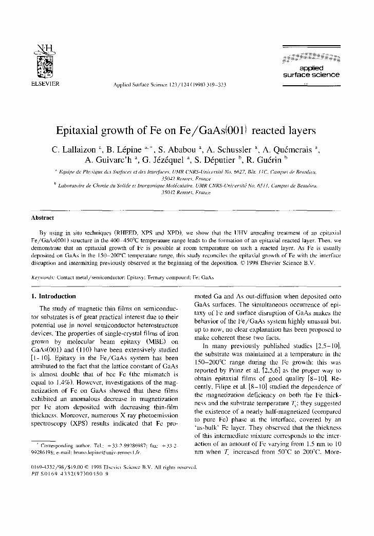
Fig. 1. RHEED pattern along the [110] azimuth of the GaAs substrate: (a) on the starting (2 × 4) GaAs(001) surface, (b) after a 6 nm thick Fe deposition at RT, (c) after UHV annealing of the structure at 400°C during 15 rain, and (d) after another Fe deposition (10 nm thick) at RT.
C. Lallaizon et al./Applied Surjace Science 123 / 124 (1998) 319-323 321
energy diffraction (RHEED) and connected to an analysis chamber by a UHV modutrack system. Un- doped GaAs buffer layers (500 nm thick and As 2 × 4 terminated) were grown on n +-type GaAs(001) substrates using standard MBE conditions. Fe depo- sitions were perlbrmed at RT in the analysis cham- ber using a deposition rate of 0.2 nm min ~ using an effusion cell. The various stages of formation of the Fe/Reacted layer/GaAs(001) structure were moni- tored by RHEED, X-ray photoemission spectroscopy (XPS) (using Mg Kc~ radiation) and X-ray photo- electron diffraction (XPD). The photoemission inten- sity distributions were recorded as a function of the polar angle in the [100] GaAs azimuth. The angular resolution was better than 3 ° .
3. Results
Fig. la shows the RHEED pattern of the starting (2 × 4) GaAs(001) surface, along the [110] azimuth.
After a 6 nm thick Fe deposition at room tempera- ture (Fig. lb), the RHEED pattern is in agreement with the epitaxial growth of bcc Fe with a (001) surface and the in-plane [100] axes of Fe and GaAs aligned [5]. The surface is unreconstructed and the discontinuity of the streaks denotes a rather three-di- mensional growth of Fe. When the Fe film is an- nealed, the RHEED pattern begins to evolve at 300°C. The streaks become continuous and additional lines appear in the ½ position leading to the characteristic diagram shown in Fig. lc at 400°C. Since no recon- struction is expected on pure Fe by heat treatment, this result suggests the out-diffusion of Ga a n d / o r As atoms up to the surface. This out-diffusion results into an ordered reacted layer much smoother at the surface than the as deposited Fe film. Another Fe deposition (10 nm thick) at RT on this reacted layer leads to a RHEED pattern (Fig. l d) quite similar to the one obtained for as deposited Fe layer directly on GaAs substrate.
e-
e" m
Ga 3d
(a) i
_J I '
L (c)
1224 1228
As 3d Fe 3p
(
I ' I , I
i
1204 12'08
Kinetic energy (eV)
, . , . , . , . , . ,
< I I I I I I
188 1 4 9 2 1496
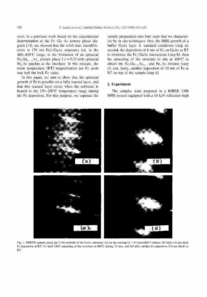
Fig. 2. Ga3d, AS3d or Fe3p photoemission spectra: (a) of the starting (2 × 4) (001 )GaAs surface, (b) of a 6 nm thick Fe deposition at RT, (c) after UHV annealing of the sample at 400°C during 15 min.
322 C. Lallaizon et al. / Applied Surjace Science 123/124 (1998) 319-323
The XPS analysis of the surface at various stages of the sample preparation is reported in Fig. 2. Alter the 6 nm thick Fe deposition (Fig. 2b), the Ga3a and As3a components from the substrate are no more visible. Fe covers the whole GaAs surface. However, a very small amount of As can be detected at the surface (not shown here). Alter the 400°C annealing (Fig. 2c), both Ga3d and AS3d c o r e levels reappear but are shifted with respect to the GaAs position. Ga3a core level consists of a single component, its position is 1 eV shifted towards lower binding en- ergy. AS3d c o r e level consists of two components, one is shifted towards lower binding energy, the other towards higher binding energy. After normali- sation by the photoionization cross-section calculated by Scofield [12], the integrated intensities of the Ga3d and As3a components are of the same order of magnitude as the Fe3p core level component, point- ing out a strong intermixing between the three species.
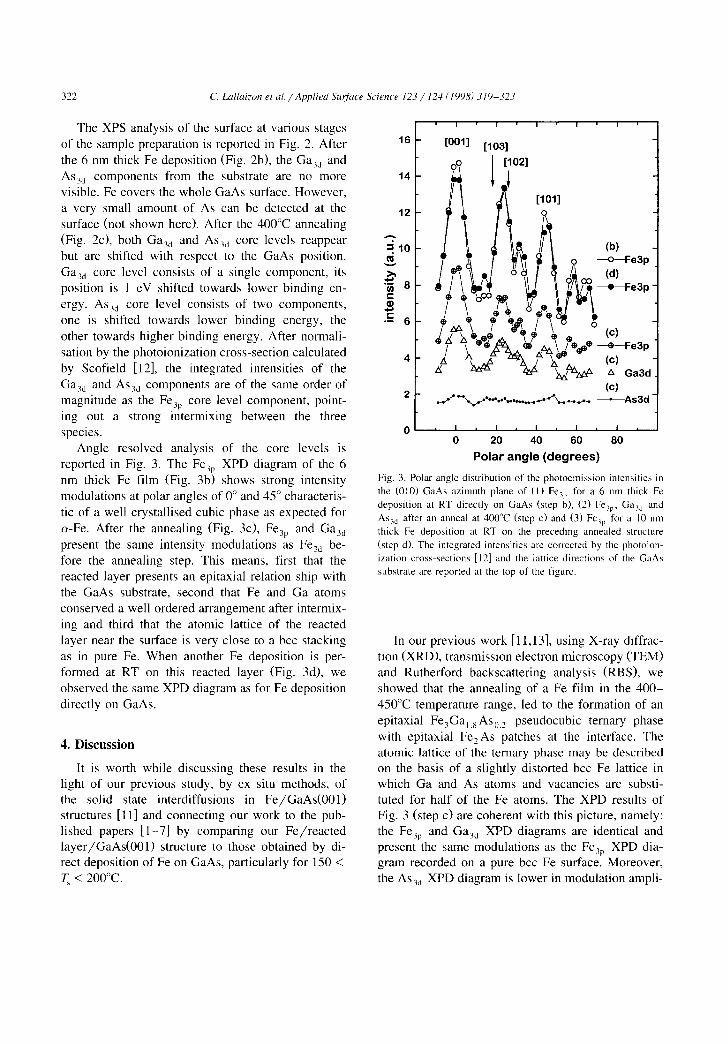
Angle resolved analysis of the core levels is reported in Fig. 3. The Fe3p XPD diagram of the 6 nm thick Fe film (Fig. 3b) shows strong intensity modulations at polar angles of 0 ° and 45 ° characteris- tic of a well crystallised cubic phase as expected for ce-Fe. After the annealing (Fig. 3c), Fe3p and Ga3d present the same intensity modulations as Fe3d be- fore the annealing step. This means, first that the reacted layer presents an epitaxial relation ship with the GaAs substrate, second that Fe and Ga atoms conserved a well ordered arrangement after intermix- ing and third that the atomic lattice of the reacted layer near the surface is very close to a bcc stacking as in pure Fe. When another Fe deposition is per- formed at RT on this reacted layer (Fig. 3d), we observed the same XPD diagram as for Fe deposition directly on GaAs.
4. Discussion
It is worth while discussing these results in the light of our previous study, by ex situ methods, of the solid state interdiffusions in Fe/GaAs(001) structures [11] and connecting our work to the pub- lished papers [1-7] by comparing our Fe/reacted layer/GaAs(001) structure to those obtained by di- rect deposition of Fe on GaAs, particularly for 150 < T~ < 200°C.
16
14
12
A
=.1o
"3 8 e-
.E 6
o o 20 40 60 80
Polar angle (degrees)
Fig. 3. Polar angle distribution of the photoemission intensities in the (010) GaAs azimuth plane of (1) Fe3p for a 6 nm thick Fe deposition at RT directly on GaAs (step b), (2) Fe3p, Ga3d and As3d after an anneal at 400°C (step c) and (3) Fe3p for a 10 nm thick Fe deposition at RT on the preceding annealed structure (step d). The integrated intensities are corrected by the photoion- ization cross-sections [12] and the lattice directions of the GaAs substrate are reported at the top of the figurc.
In our previous work [11,13], using X-ray diffrac- tion (XRD), transmission electron microscopy (TEM) and Rutherford backscattering analysis (RBS), we showed that the annealing of a Fe film in the 400- 450°C temperature range, led to the formation of an epitaxial Fe3Gal8Aso 2 pseudocubic ternary phase with epitaxial Fe2As patches at the interface. The atomic lattice of the ternary phase may be described on the basis of a slightly distorted bcc Fe lattice in which Ga and As atoms and vacancies are substi- tuted for half of the Fe atoms. The XPD results of Fig. 3 (step c) are coherent with this picture, namely: t h e Fe3p and Ga3d XPD diagrams are identical and present the same modulations as the Fe3p XPD dia- gram recorded on a pure bcc Fe surface. Moreover, the As3a XPD diagram is lower in modulation ampli-
C. Lallaizon et al./Applied Surface Science 123 / 124 (1998) 319-323 323
tude and mean value than the one of Ga3d; this is again in agreement with the low As composition of the ternary compound that we found and the fact that the As rich compound Fe2As is slightly buried. In conclusion, our results show that the annealing of a Fe/GaAs structure leads to the formation of an epitaxial reacted layer identified, at the surface, as the Fe3Gal. s As02 phase which promotes an epitaxial regrowth of Fe. In this way, we demonstrate that a disruption of the GaAs surface involving strong in- termixing is fully compatible with an Fe epitaxial growth.
In addition, we recently performed an XPS study of a sequential deposition of Fe on GaAs at iV, = 200°C. Our results show the formation of a Fe/re- acted layer/GaAs structure quite similar to the one we discussed in the previous paragraph. The Ga3d and As3d core level line shapes are very similar and the XRD measurements are also compatible with the presence of the Fe3GatsAs0.2 and FezAs com- pounds. In this case, the reacted layer corresponds to the interaction of a 7 nm Fe film with GaAs.
5. Conclusion
The scheme we use in this study, namely separat- ing reaction step from Fe growth step, associated with in situ characterization and especially angle resolved X-ray photoemission, allows to give a twofold conclusion. The epitaxial growth of Fe is
possible on the reacted layer resulting from the annealing of an Fe/GaAs structure. The epitaxial Fe growth that is obtained on heated GaAs substrate consists also of an Fe layer on top of a reacted layer, whose nature is comparable to the previous one. We have obtained in this way a clear and uniform de- scription of the epitaxial Fe/GaAs contacts.
References
[1] J.R. Waltrop, R.W. Grant, Appl. Phys. Lett. 34 (1979) 630. [2] G.A. Prinz, J.J. Krebs, Appl. Phys. Lett. 39 (1981) 397. [3] M.W. Ruckman, J.J. Joyce, J.H. Weaver, Phys. Rev. B 33
(1986) 7029. [4] S.A. Chambers, F. Xu, H.W. Chen, I.M. Vitomirov, S.B,
Anderson, J.H. Weaver, Phys. Rev. B 34 (1986) 6605. [5] J.J. Kreps, B.T. Jonker, G.A. Prinz, J. Appl. Phys. 61 (1987)
2596. [6] G.A. Prinz, in: Uhrathin Magnetic Structures, vol. I1,
Springer, 1994, p. 144. [7] E. Kneedler, P.M. Thibado, B.T. Jonker, B.R. Bennett. B.V,
Shanabrook, R.J. Wagner, L.L Whitman, J. Vac. Sci. Tech- nol. B 14 (1996) 3193.
[8] A. Filipe, A. Schuhl, P. Galtier, Appl. Phys. Lett. 70 (1997) 129.
[9] A. Filipe, A. Schuhl, J. Appl. Phys. 81 (1997) 4359. [10] A. Filipe, Thesis, Ecole Polytechnique, Palaiseau, 1997. [11] S. D6putier, R. Gudrin, B. L~pine, A. Guivarc'h, G. Jdz6quel,
J. Alloys Comp., in press. [12] J.H. Scofield. J. Electron Spectrosc. 8 (1976) 129. [13] B. L6pine, S. Ababou, A. Guivarc'h, G. J6z6quel, S. D6pu-
tier, R. GuErin, A. Filipe, A. Schuhl, F. Abel, C. Cohen, A. Rocher, J. Crestou, J. Appl. Phys., in press.