Embed Size (px)
Citation preview
Thin Solid Films 545 (2013) 302–309
Contents lists available at ScienceDirect
Thin Solid Films
j ourna l homepage: www.e lsev ie r .com/ locate / ts f
Fluorine-doped SnO2 thin films deposited on polymer substrate forflexible transparent electrodes
A. Muthukumar a,b, G. Giusti a,⁎, M. Jouvert a, V. Consonni a, D. Bellet a
a Laboratoire des Matériaux et du Génie Physique, Grenoble INP, CNRS, Grenoble 38016, Franceb Crystal Growth Centre, Anna University, Chennai 600025, India
⁎ Corresponding author.E-mail address: [email protected] (G. Giusti).
0040-6090/$ – see front matter © 2013 Elsevier B.V. All rihttp://dx.doi.org/10.1016/j.tsf.2013.08.085
a b s t r a c t
a r t i c l e i n f oArticle history:Received 5 January 2013Received in revised form 21 August 2013Accepted 23 August 2013Available online 31 August 2013
Keywords:Flexible substrateTransparent conductorSpray pyrolysisTin dioxide filmsTexture
Fluorine-doped SnO2 (FTO) thin films are deposited by ultrasonic spray pyrolysis on preheated polyimide (PI)substrates. Their structural, electro-optical and electro-mechanical properties are investigated versus bothgrowth temperature and film thickness. FTO thin films exhibit textured columnar grain morphology and pre-ferred orientations along the b101N, b301N, b211N and b200N are favored depending on growth temperatureand film thickness. The films deposited on PI substrate at 380 °C present the best compromise in terms ofelectro-optical properties with a low electrical resistivity of 8.9 × 10⁻⁴ Ω cm, a mobility of 17.9 cm2/V·s com-bined with an optical transmittance up to 79.4% at 780 nm. Eventually, a figure of merit of 2.3 × 10⁻³Ω−1 isobtained. The electro-mechanical properties are studied during controlled fatigue testing and analyzed accordingto the energy-based Griffith's criterion.
© 2013 Elsevier B.V. All rights reserved.
1. Introduction
Transparent conductive oxides (TCO) are wide band gap semi-conductors combining high optical transmittance (up to 90%) withlow electrical resistivity (i.e. a few times 10−4 Ω cm). They havebeen extensively studied over the past few decades and still main-tain a dominant role in opto-electronic devices as transparent elec-trodes [1,2]. However, the growing need for flexible devices makesflexible transparent electrodes increasingly attractive due to theirlower cost, lightweight, mechanical flexibility and amenability toroll-to-roll fabrication as compared with their variant used on rigidglass substrates. Such flexible transparent electrodes can be used insolar cells [3,4], organic light emitting devices [5–7] or plastic liquidcrystal displays [8,9]. Their use in flexible devices has been reviewedin Ref. [10]. In parallel, dielectric/metal/dielectric systems haveproven to be very promising candidates for transparent electrodes[11–15]. It consists in sandwiching a metallic layer in between twoTCO layers. Recently, multilayers of indium zinc oxide (IZO) and silverhave even been grown on polyethylene terephtalate (PET) substrateusing roll-to-roll sputtering [16]. Interestingly, such interlayers candrastically improve crack and buckling delamination resistances [17].
Until now, a wide range of TCO films have been grown on polymersubstrates by sputtering such as IZO [18,19], aluminium zinc oxide(AZO) [20] and indium tin oxide (ITO) [21–24]. High quality crystallineITO films have also been deposited by pulsed-laser deposition [25,26].
ghts reserved.
For example, Kim et al. have obtained an electrical resistivity as low as10−4 Ω cm and an average transmittance of 90% in the visible rangeat the substrate temperature of 100 °C [25]. Socol et al. [27] have recentlyreported similar results on IZO, AZO and ITO thin films grown on PETsubstrates using the same technique. Low pressure metal organicchemical vapor deposition has also been used for depositing boron-doped ZnO thin films directly on PET substrates [4].
Concerning more specifically tin dioxide, it interestingly exhibitshigher chemical and mechanical stability than ITO [28]. High qualityfluorine-doped tin oxide (FTO) layers can be grown by spray pyroly-sis at about 400 °C. Spray pyrolysis offers several advantages amongwhich cost effectiveness, ease of doping and large-area coating abil-ity [29]. Using such technique, Huang et al. [30] have reported a re-sistivity of 7.6 × 10⁻⁴ Ω cm for FTO thin films first grown on brasssubstrates by spray pyrolysis and then cemented on a PET substrate.Since growth takes place on compliant substrates, the mechanicalproperties of such layers are of prime importance. They have beenextensively reviewed by Chen et al. [31,32] and Cotterell et al. [33].Basically, when a thin film deposited on a flexible substrate isunder tension, channeling cracks going through the film first appearallowing partial relaxation of stress, eventually followed by bucklingdelamination. Under compression, the situation is reversed: thecoating first delaminates and buckles before cracking.
In thiswork, high thermal stability Kapton© substrates (Kapton©PV9101, DuPont® Company) are used. The prime aim of this work is togrow transparent conductive FTO layers on flexible substrate and to in-vestigate their physical properties as a function of both growth temper-ature and film thickness.
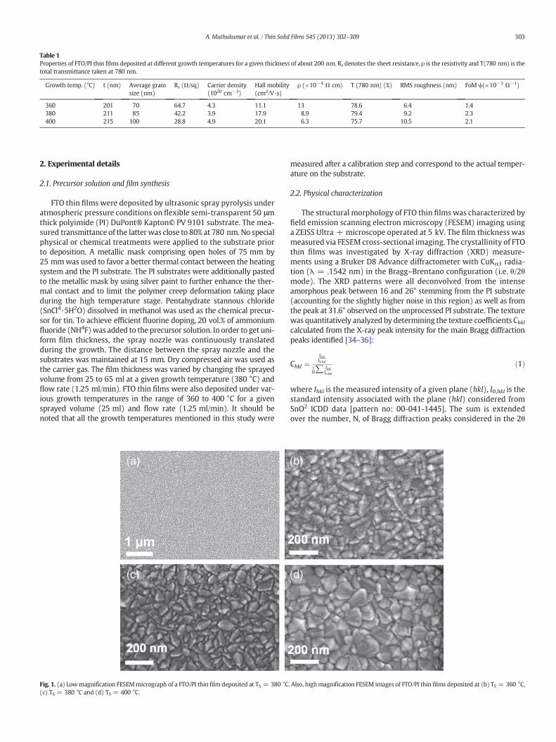
Table 1Properties of FTO/PI thin films deposited at different growth temperatures for a given thickness of about 200 nm. Rs denotes the sheet resistance, ρ is the resistivity and T(780 nm) is thetotal transmittance taken at 780 nm.
Growth temp. (°C) t (nm) Average grainsize (nm)
Rs (Ω/sq) Carrier density(1020 cm−3)
Hall mobility(cm2/V·s)
ρ (×10−4 Ω cm) T (780 nm) (%) RMS roughness (nm) FoM ψ(×10−3 Ω−1)
360 201 70 64.7 4.3 11.1 13 78.6 6.4 1.4380 211 85 42.2 3.9 17.9 8.9 79.4 9.2 2.3400 215 100 28.8 4.9 20.1 6.3 75.7 10.5 2.1
303A. Muthukumar et al. / Thin Solid Films 545 (2013) 302–309
2. Experimental details
2.1. Precursor solution and film synthesis
FTO thin films were deposited by ultrasonic spray pyrolysis underatmospheric pressure conditions on flexible semi-transparent 50 μmthick polyimide (PI) DuPont® Kapton© PV 9101 substrate. The mea-sured transmittance of the latter was close to 80% at 780 nm. No specialphysical or chemical treatments were applied to the substrate priorto deposition. A metallic mask comprising open holes of 75 mm by25 mmwas used to favor a better thermal contact between the heatingsystem and the PI substrate. The PI substrates were additionally pastedto the metallic mask by using silver paint to further enhance the ther-mal contact and to limit the polymer creep deformation taking placeduring the high temperature stage. Pentahydrate stannous chloride(SnCl4·5H2O) dissolved in methanol was used as the chemical precur-sor for tin. To achieve efficient fluorine doping, 20 vol.% of ammoniumfluoride (NH4F)was added to the precursor solution. In order to get uni-form film thickness, the spray nozzle was continuously translatedduring the growth. The distance between the spray nozzle and thesubstrates was maintained at 15 mm. Dry compressed air was used asthe carrier gas. The film thickness was varied by changing the sprayedvolume from 25 to 65 ml at a given growth temperature (380 °C) andflow rate (1.25 ml/min). FTO thin films were also deposited under var-ious growth temperatures in the range of 360 to 400 °C for a givensprayed volume (25 ml) and flow rate (1.25 ml/min). It should benoted that all the growth temperatures mentioned in this study were
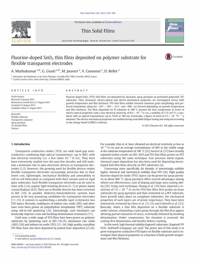
(a)
(c)
Fig. 1. (a) Lowmagnification FESEMmicrograph of a FTO/PI thin film deposited at TS = 380 °C(c) TS = 380 °C and (d) TS = 400 °C.
measured after a calibration step and correspond to the actual temper-ature on the substrate.
2.2. Physical characterization
The structural morphology of FTO thin films was characterized byfield emission scanning electron microscopy (FESEM) imaging usinga ZEISS Ultra + microscope operated at 5 kV. The film thickness wasmeasured via FESEM cross-sectional imaging. The crystallinity of FTOthin films was investigated by X-ray diffraction (XRD) measure-ments using a Bruker D8 Advance diffractometer with CuKα1 radia-tion (λ = .1542 nm) in the Bragg–Brentano configuration (i.e. θ/2θmode). The XRD patterns were all deconvolved from the intenseamorphous peak between 16 and 26° stemming from the PI substrate(accounting for the slightly higher noise in this region) as well as fromthe peak at 31.6° observed on the unprocessed PI substrate. The texturewas quantitatively analyzed by determining the texture coefficients Chklcalculated from the X-ray peak intensity for the main Bragg diffractionpeaks identified [34–36]:
Chkl ¼IhklI0;hkl
1N∑ Ihkl
I0;hkl
ð1Þ
where Ihkl is the measured intensity of a given plane (hkl), I0,hkl is thestandard intensity associated with the plane (hkl) considered fromSnO2 ICDD data [pattern no: 00-041-1445]. The sum is extendedover the number, N, of Bragg diffraction peaks considered in the 2θ
(b)
(d)
. Also, highmagnification FESEM images of FTO/PI thin films deposited at (b) TS = 360 °C,
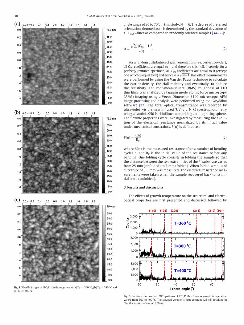
Fig. 2. 3D AFM images of FTO/PI thin films grown at (a) TS = 360 °C, (b) TS = 380 °C and(c) TS = 400 °C.
304 A. Muthukumar et al. / Thin Solid Films 545 (2013) 302–309
angle range of 20 to 70°. In this study, N = 6. The degree of preferredorientation, denoted as σ, is determined by the standard deviation ofall Chkl values as compared to randomly oriented samples [34–36]:
σ ¼ffiffiffiffiffiffiffiffiffiffiffiffiffiffiffiffiffiffiffiffiffiffiffiffiffiffiffiffi∑ Chkl−1ð Þ2
qffiffiffiffiN
p : ð2Þ
For a random distribution of grain orientations (i.e. perfect powder),all Chkl coefficients are equal to 1 and therefore σ is null. Inversely, for aperfectly textured specimen, all Chkl coefficients are equal to 0 (exceptonewhich is equal to N) and henceσ is
ffiffiffiffiffiffiffiffiffiffiffiN−1
p. Hall effectmeasurements
were performed by using the Van der Pauw technique to calculatethe carrier density, the Hall mobility and eventually, to deducethe resistivity. The root-mean-square (RMS) roughness of FTOthin films was analyzed by tapping mode atomic force microscopy(AFM) imaging using a Veeco Dimension 3100 microscope. AFMimage processing and analysis were performed using the Gwyddionsoftware [37]. The total optical transmittance was recorded byultraviolet–visible-near infrared (UV–vis–NIR) spectrophotometryusing a Lambda 950 PerkinElmer comprising an integrating sphere.The flexible properties were investigated by measuring the evolu-tion of the electrical resistance normalized by its initial valueunder mechanical constraints. F(n) is defined as:
F nð Þ ¼ R nð ÞR0
ð3Þ
where R(n) is the measured resistance after a number of bendingcycles n, and R0 is the initial value of the resistance before anybending. One folding cycle consists in folding the sample so thatthe distance between the two extremities of the PI substrate variesfrom 25 mm (unfolded) to 7 mm (folded). When folded, a radius ofcurvature of 3.5 mm was measured. The electrical resistance mea-surements were taken when the sample recovered back to its ini-tial state (unfolded).
3. Results and discussions
The effects of growth temperature on the structural and electro-optical properties are first presented and discussed, followed by
Fig. 3. Substrate deconvolved XRD patterns of FTO/PI thin films as growth temperaturevaried from 360 to 400 °C. The sprayed volume is kept constant (25 ml) resulting infilm thicknesses of around 200 nm.
nsm
itta
nce
(%
)
40
60
80
100
305A. Muthukumar et al. / Thin Solid Films 545 (2013) 302–309
the electro-mechanical properties. The same procedure is consid-ered for the effects of film thickness.
3.1. Growth temperature effects on textured FTO/PI thin film growth
Table 1 sums up the structural, electrical and optical properties ofFTO thin films on PI substrate (FTO/PI) deposited at various temper-atures for an average film thickness of around 200 nm. A figure ofmerit (FoM) is calculated for each sample to assess under which con-ditions the best compromise in terms of electro-optical properties isachieved. This compromise is often associated with maximizing theFoM defined as [38]: FoM = T10/Rs, where T is the optical transmit-tance and Rs is the sheet resistance. In this study, the FoM calculationwas conducted by taking the total transmittance measured at780 nm instead of 550 nm (as usually reported) owing to the semi-opacity of the PI substrate below this wavelength.
The structuralmorphology of FTO/PI thin films is presented in Figs. 1and 2 by FESEMmicrographs and three dimensional (3D) AFM imaging,respectively.
The grain structure appears compact and no crack is observed forthe as deposited specimens. The average grain size increases from 70to 100 nm as growth temperature is raised from 360 to 400 °C, as re-vealed by the top-view FESEM image analysis (See Fig. 1). Further-more, the grains of the film at 400 °C develop much better definedfacets than at 360 °C. This could be attributed to grain size effectscombined with enhanced chemical etching of the film surface duringgrowth at higher temperature owing to the corrosive atmosphereunder which growth takes place [39]. The RMS roughness also in-creases with growth temperature from 6.4 nm to 10.5 nm between360 and 400 °C alongwith the average grain size as expected in poly-crystalline thin films. The increase in grain size can be accounted forthe thermal activation of grain boundary migration at the surface ofthe growing film as growth temperature is raised.
The structural properties of the layers are further investigated byXRD. The XRD patterns of FTO/PI thin films deposited at differentgrowth temperatures are shown in Fig. 3. The films fit well with thepolycrystalline SnO2 cassiterite phase, tetragonal crystal structure.No sign of the presence of the SnO phase is made and the texture co-efficients and the degree of preferred orientation are calculated andsummarized in Table 2.
The degree of preferred orientation in the range of 0.4 to 0.6 isfairly low and does not vary significantly within the growth temper-ature range. Concerning the texture coefficients, the lowest growthtemperature favors the b101N, b301N and b200N crystallographic di-rections while the highest growth temperature makes the b211N,b301N and b200N directions more predominant. The growth temper-ature dependent texture can be understood via the process of abnor-mal grain growth for which grain growth proceeds to minimize thetotal free energy [35,36,40]. Our results are in relative agreement withthe experimental results reported by Consonni et al. [36] for FTO thinfilms deposited on glass substrate under similar growth conditions.From Ref. [36], it is expected that the b101N preferred orientation arisesfrom surface energy minimization as the reduced (101) surfacepresents the lowest surface energy for low growth temperature. Incontrast, the b200N and b301N orientations are related to strain energyminimization [35,36].
Table 2Degree of preferred orientation (σ) and texture coefficients (Chkl) as a function of growthtemperature for a given film thickness of about 200 nm.
Growthtemperature (°C)
Degree of preferredorientation (σ)
C110 C101 C200 C211 C310 C301
360 0.60 0.86 1.81 1.47 1.18 0.04 1.54380 0.46 0.41 0.99 1.70 1.45 0.60 1.25400 0.49 0.33 0.98 1.45 1.55 0.52 1.48
However, it should be noted that the difference in roughness aswell as bonding strength between the thin film on one side and theCorning glass or PI substrates on the other side could give rise to dif-ferent growth modes. In this situation, the interface energy mayslightly affect the thermodynamic considerations used in Refs.[35,36,41]. Moreover, the difference in thermal expansion coeffi-cients (3.8 × 10⁻⁶/°C and 12.0 × 10⁻⁶/°C for the Corning glass andthe PI substrate, respectively) might result in a change in elasticstrain energy density for the corresponding layers [35,36].
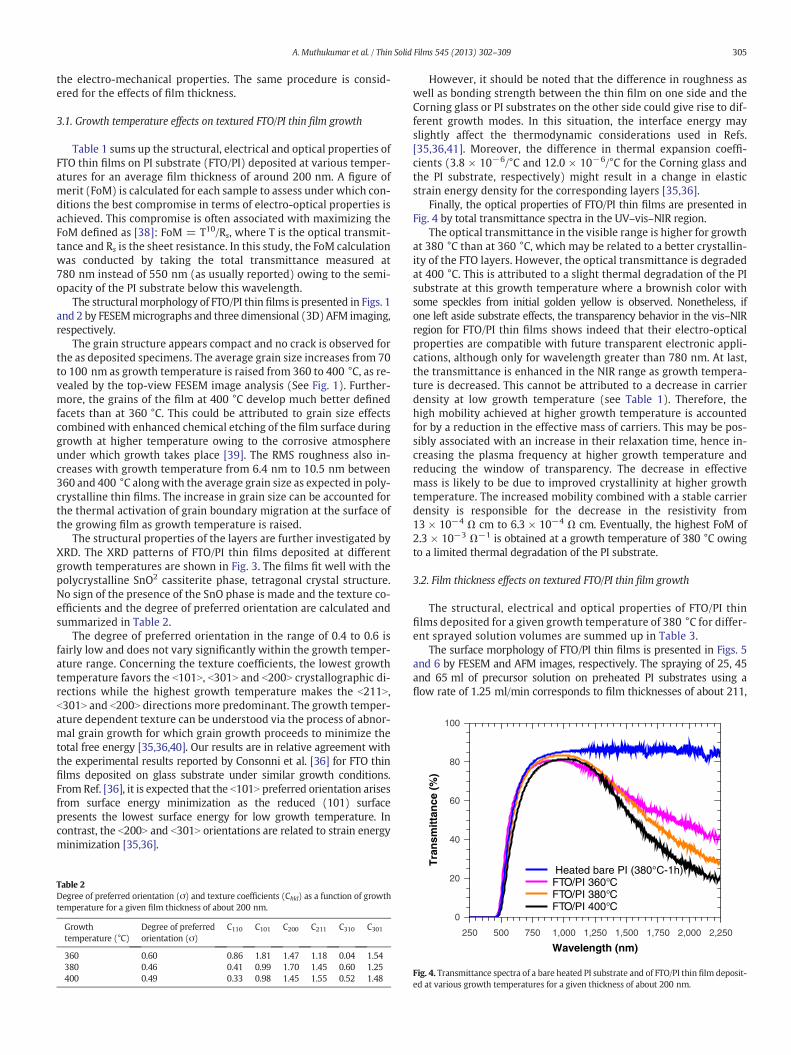
Finally, the optical properties of FTO/PI thin films are presented inFig. 4 by total transmittance spectra in the UV–vis–NIR region.
The optical transmittance in the visible range is higher for growthat 380 °C than at 360 °C, which may be related to a better crystallin-ity of the FTO layers. However, the optical transmittance is degradedat 400 °C. This is attributed to a slight thermal degradation of the PIsubstrate at this growth temperature where a brownish color withsome speckles from initial golden yellow is observed. Nonetheless, ifone left aside substrate effects, the transparency behavior in the vis–NIRregion for FTO/PI thin films shows indeed that their electro-opticalproperties are compatible with future transparent electronic appli-cations, although only for wavelength greater than 780 nm. At last,the transmittance is enhanced in the NIR range as growth tempera-ture is decreased. This cannot be attributed to a decrease in carrierdensity at low growth temperature (see Table 1). Therefore, thehigh mobility achieved at higher growth temperature is accountedfor by a reduction in the effective mass of carriers. This may be pos-sibly associated with an increase in their relaxation time, hence in-creasing the plasma frequency at higher growth temperature andreducing the window of transparency. The decrease in effectivemass is likely to be due to improved crystallinity at higher growthtemperature. The increased mobility combined with a stable carrierdensity is responsible for the decrease in the resistivity from13 × 10−4 Ω cm to 6.3 × 10⁻⁴ Ω cm. Eventually, the highest FoM of2.3 × 10−3 Ω−1 is obtained at a growth temperature of 380 °C owingto a limited thermal degradation of the PI substrate.
3.2. Film thickness effects on textured FTO/PI thin film growth
The structural, electrical and optical properties of FTO/PI thinfilms deposited for a given growth temperature of 380 °C for differ-ent sprayed solution volumes are summed up in Table 3.
The surface morphology of FTO/PI thin films is presented in Figs. 5and 6 by FESEM and AFM images, respectively. The spraying of 25, 45and 65 ml of precursor solution on preheated PI substrates using aflow rate of 1.25 ml/min corresponds to film thicknesses of about 211,
Tra
0
20
Wavelength (nm)250 500 750 1,000 1,250 1,500 1,750 2,000 2,250
Heated bare PI (380°C-1h)FTO/PI 360°CFTO/PI 380°CFTO/PI 400°C
Fig. 4. Transmittance spectra of a bare heated PI substrate and of FTO/PI thin film deposit-ed at various growth temperatures for a given thickness of about 200 nm.
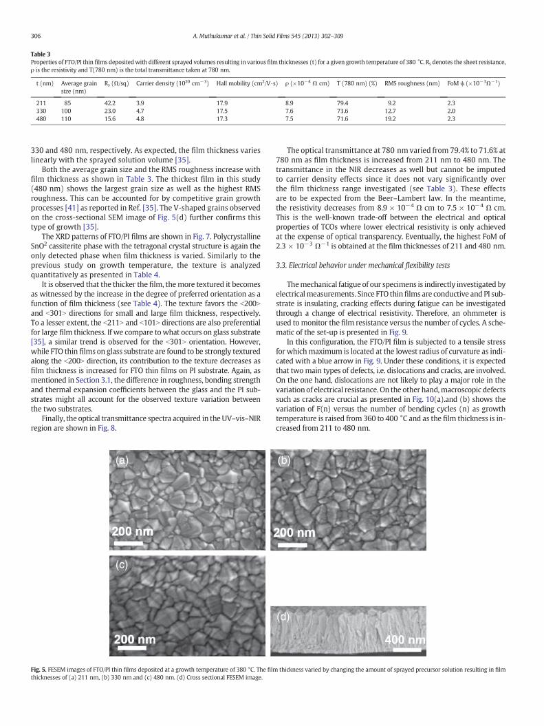
Table 3Properties of FTO/PI thin films depositedwith different sprayed volumes resulting in various film thicknesses (t) for a given growth temperature of 380 °C. Rs denotes the sheet resistance,ρ is the resistivity and T(780 nm) is the total transmittance taken at 780 nm.
t (nm) Average grainsize (nm)
Rs (Ω/sq) Carrier density (1020 cm−3) Hall mobility (cm2/V·s) ρ (×10−4 Ω cm) T (780 nm) (%) RMS roughness (nm) FoM ψ (×10−3Ω−1)
211 85 42.2 3.9 17.9 8.9 79.4 9.2 2.3330 100 23.0 4.7 17.5 7.6 73.6 12.7 2.0480 110 15.6 4.8 17.3 7.5 71.6 19.2 2.3
306 A. Muthukumar et al. / Thin Solid Films 545 (2013) 302–309
330 and 480 nm, respectively. As expected, the film thickness varieslinearly with the sprayed solution volume [35].
Both the average grain size and the RMS roughness increase withfilm thickness as shown in Table 3. The thickest film in this study(480 nm) shows the largest grain size as well as the highest RMSroughness. This can be accounted for by competitive grain growthprocesses [41] as reported in Ref. [35]. The V-shaped grains observedon the cross-sectional SEM image of Fig. 5(d) further confirms thistype of growth [35].
The XRD patterns of FTO/PI films are shown in Fig. 7. PolycrystallineSnO2 cassiterite phase with the tetragonal crystal structure is again theonly detected phase when film thickness is varied. Similarly to theprevious study on growth temperature, the texture is analyzedquantitatively as presented in Table 4.
It is observed that the thicker the film, themore textured it becomesas witnessed by the increase in the degree of preferred orientation as afunction of film thickness (see Table 4). The texture favors the b200Nand b301N directions for small and large film thickness, respectively.To a lesser extent, the b211N and b101N directions are also preferentialfor large film thickness. If we compare to what occurs on glass substrate[35], a similar trend is observed for the b301N orientation. However,while FTO thin films on glass substrate are found to be strongly texturedalong the b200N direction, its contribution to the texture decreases asfilm thickness is increased for FTO thin films on PI substrate. Again, asmentioned in Section 3.1, the difference in roughness, bonding strengthand thermal expansion coefficients between the glass and the PI sub-strates might all account for the observed texture variation betweenthe two substrates.
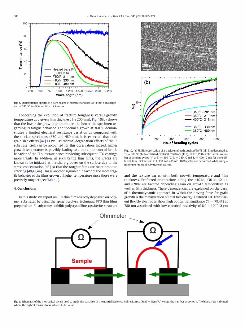
Finally, the optical transmittance spectra acquired in theUV–vis–NIRregion are shown in Fig. 8.
(a)
(c)
Fig. 5. FESEM images of FTO/PI thin films deposited at a growth temperature of 380 °C. The filmthicknesses of (a) 211 nm, (b) 330 nm and (c) 480 nm. (d) Cross sectional FESEM image.
The optical transmittance at 780 nm varied from 79.4% to 71.6% at780 nm as film thickness is increased from 211 nm to 480 nm. Thetransmittance in the NIR decreases as well but cannot be imputedto carrier density effects since it does not vary significantly overthe film thickness range investigated (see Table 3). These effectsare to be expected from the Beer–Lambert law. In the meantime,the resistivity decreases from 8.9 × 10⁻⁴ Ω cm to 7.5 × 10⁻⁴ Ω cm.This is the well-known trade-off between the electrical and opticalproperties of TCOs where lower electrical resistivity is only achievedat the expense of optical transparency. Eventually, the highest FoM of2.3 × 10−3 Ω−1 is obtained at the film thicknesses of 211 and 480 nm.
3.3. Electrical behavior under mechanical flexibility tests
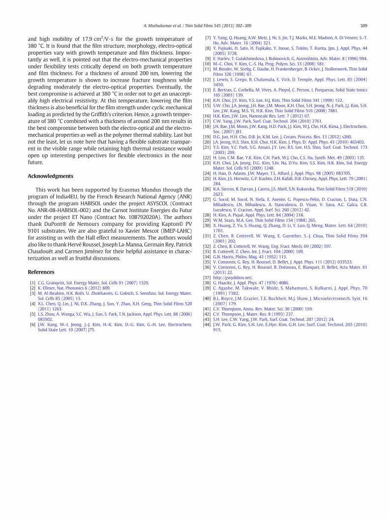
Themechanical fatigue of our specimens is indirectly investigated byelectricalmeasurements. Since FTO thinfilms are conductive and PI sub-strate is insulating, cracking effects during fatigue can be investigatedthrough a change of electrical resistivity. Therefore, an ohmmeter isused tomonitor the film resistance versus the number of cycles. A sche-matic of the set-up is presented in Fig. 9.
In this configuration, the FTO/PI film is subjected to a tensile stressfor whichmaximum is located at the lowest radius of curvature as indi-cated with a blue arrow in Fig. 9. Under these conditions, it is expectedthat twomain types of defects, i.e. dislocations and cracks, are involved.On the one hand, dislocations are not likely to play a major role in thevariation of electrical resistance. On the other hand,macroscopic defectssuch as cracks are crucial as presented in Fig. 10(a).and (b) shows thevariation of F(n) versus the number of bending cycles (n) as growthtemperature is raised from 360 to 400 °C and as the film thickness is in-creased from 211 to 480 nm.
(b)
(d)
thickness varied by changing the amount of sprayed precursor solution resulting in film
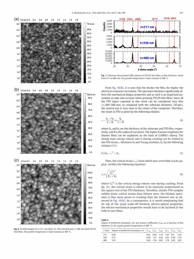
Fig. 6. 3D AFM images of (a) 211 nm thick, (b) 330 nm thick and (c) 480 nm thick FTO/PIthin films. The growth temperature is kept constant at 380 °C.
Fig. 7. Substrate deconvolved XRD patterns of FTO/PI thin films as film thickness variedfrom 211 to 480 nm. The growth temperature is kept constant at 380 °C.
307A. Muthukumar et al. / Thin Solid Films 545 (2013) 302–309
From Fig. 10(b), it is seen that the thicker the film, the higher theelectrical resistance increment. The specimen thickness significantly af-fects the mechanical fatigue properties and as such is an important pa-rameter to take into account when growing FTO/PI thin films. Since allthe FTO layers reported in this work can be considered very thin(≈200–500 nm) as compared with the substrate thickness (50 μm),the neutral axis is very close to the center of the composite. Therefore,the strain in FTO is given by the following relation:
� ¼ hs þ hf
2� R≈ hs
2� Rð4Þ
where hs and hf are the thickness of the substrate and FTO film, respec-tively, and R is the radius of curvature. The higher fracture toughness forthinner films can be explained on the basis of Griffith's theory. Thesteady state energy release rate G during cracking can be related tothe FTO strain �, thickness hf and Youngmodulus, Ef, by the followingrelation [31]:
G∝Ef � �2 � hf : ð5Þ
Then, the critical strain (�c), fromwhich non-reversible cracks ap-pear, verifies the following equation:
�c∝
ffiffiffiffiffiffiffiffiffiffiffiffiffiffiffiffiGcritc
Ef � hf
sð6Þ
where Gccrit is the critical energy release rate during cracking. From
Eq. (6), the critical strain is shown to be inversely proportional tothe square root of the FTO thickness. Therefore, thicker FTO samplesexhibit lower critical strains than thinner ones: the thickest speci-men is thus more prone to cracking than the thinnest one as ob-served in Fig. 10(b). As a consequence, it is worth mentioning thaton top of the usual trade-off between electro-optical properties,the electro-mechanical properties would have to be factored in theFoM of such films.
Table 4Degree of preferred orientation (σ) and texture coefficients (Chkl) as a function of filmthickness (t) for a given growth temperature of 380 °C.
t (nm) Degree of preferred orientation (σ) C110 C101 C200 C211 C310 C301
211 0.46 0.41 0.99 1.70 1.45 0.6 1.25330 0.71 0.39 1.91 0.42 1.83 0.30 1.52480 1.01 0.24 1.56 0.03 1.78 0.05 2.65
Tra
nsm
itta
nce
(%
)
0
20
40
60
80
100
Wavelength (nm)250 500 750 1,000 1,250 1,500 1,750 2,000 2,250
Heated bare PI (380°C-1h)
FTO/PI 211 nmFTO/PI 330 nmFTO/PI 480 nm
Fig. 8. Transmittance spectra of a bare heated PI substrate and of FTO/PI thin films depos-ited at 380 °C for different film thicknesses.
(a)
(b)
Fig. 10. (a) FESEM observation of a crack running through a FTO/PI thin film deposited atTs = 380 °C. (b) Normalized electrical resistance (F(n)) of FTO/PI thin films versus num-ber of bending cycles (n) at Ts = 360 °C, Ts = 380 °C and Ts = 400 °C and for three dif-ferent film thicknesses: 211, 330 and 480 nm. 1000 cycles are performed while using aminimum radius of curvature of 3.5 mm.
308 A. Muthukumar et al. / Thin Solid Films 545 (2013) 302–309
Concerning the evolution of fracture toughness versus growthtemperature at a given film thickness (≈200 nm), Fig. 10(b) showsthat the lower the growth temperature, the better the specimen re-garding its fatigue behavior. The specimen grown at 360 °C demon-strates a limited electrical resistance variation as compared withthe thicker specimens (330 and 480 nm). It is expected that bothgrain size effects [42] as well as thermal degradation effects of the PIsubstrate itself can be accounted for this observation. Indeed, highergrowth temperature is possibly leading to a more pronounced brittlebehavior of the PI substrate hence rendering subsequent FTO coatingsmore fragile. In addition, in such brittle thin films, the cracks areknown to be initiated at the sharp grooves on the surface due to thestress concentration [43] so that the rougher films are more prone tocracking [40,43,44]. This is another argument in favor of the more frag-ile behavior of the films grown at higher temperature since those wereprecisely rougher (see Table 1).
4. Conclusions
In this study, we report on FTO thin films directly deposited on poly-mer substrates by using the spray pyrolysis technique. FTO thin filmsprepared on PI substrates exhibit polycrystalline cassiterite structure
Fig. 9. Schematic of the mechanical bench used to study the variation of the normalized electrwhere the highest tensile stress value is to be found.
and the texture varies with both growth temperature and filmthickness. Preferred orientations along the b101N, b301N, b211Nand b200N are favored depending again on growth temperature aswell as film thickness. These dependencies are explained on the basisof a thermodynamic approach in which the driving force for graingrowth is theminimization of total free energy. Textured FTO transpar-ent flexible electrodes show high optical transmittance (T = 79.4%) at780 nm associated with low electrical resistivity of 8.9 × 10⁻⁴ Ω cm
ical resistance (F(n) = R(n)/R0) versus the number of cycles n. The blue arrow indicated
309A. Muthukumar et al. / Thin Solid Films 545 (2013) 302–309
and high mobility of 17.9 cm2/V·s for the growth temperature of380 °C. It is found that the film structure, morphology, electro-opticalproperties vary with growth temperature and film thickness. Impor-tantly as well, it is pointed out that the electro-mechanical propertiesunder flexibility tests critically depend on both growth temperatureand film thickness. For a thickness of around 200 nm, lowering thegrowth temperature is shown to increase fracture toughness whiledegrading moderately the electro-optical properties. Eventually, thebest compromise is achieved at 380 °C in order not to get an unaccept-ably high electrical resistivity. At this temperature, lowering the filmthickness is also beneficial for the film strength under cyclic mechanicalloading as predicted by the Griffith's criterion. Hence, a growth temper-ature of 380 °C combined with a thickness of around 200 nm results inthe best compromise between both the electro-optical and the electro-mechanical properties as well as the polymer thermal stability. Last butnot the least, let us note here that having a flexible substrate transpar-ent in the visible range while retaining high thermal resistance wouldopen up interesting perspectives for flexible electronics in the nearfuture.
Acknowledgments
This work has been supported by Erasmus Mundus through theprogram of India4EU, by the French Research National Agency (ANR)through the program HABISOL under the project ASYSCOL (ContractNo. ANR-08-HABISOL-002) and the Carnot Institute Energies du Futurunder the project ET Nano (Contract No. 10B792020A). The authorsthank DuPont® de Nemours company for providing Kapton© PV9101 substrates. We are also grateful to Xavier Mescot (IMEP-LAHC)for assisting us with the Hall effect measurements. The authors wouldalso like to thankHervé Roussel, Joseph La-Manna, Germain Rey, PatrickChaudouët and Carmen Jiménez for their helpful assistance in charac-terization as well as fruitful discussions.
References
[1] C.G. Granqvist, Sol. Energy Mater. Sol. Cells 91 (2007) 1529.[2] K. Ellmer, Nat. Photonics 6 (2012) 809.[3] M. Al-Ibrahim, H.K. Roth, U. Zhokhavets, G. Gobsch, S. Sensfuss, Sol. Energy Mater.
Sol. Cells 85 (2005) 13.[4] X.L. Chen, Q. Lin, J. Ni, D.K. Zhang, J. Sun, Y. Zhao, X.H. Geng, Thin Solid Films 520
(2011) 1263.[5] L.S. Zhou, A. Wanga, S.C. Wu, J. Sun, S. Park, T.N. Jackson, Appl. Phys. Lett. 88 (2006)
083502.[6] J.W. Kang, W.-I. Jeong, J.-J. Kim, H.-K. Kim, D.-G. Kim, G.-H. Lee, Electrochem.
Solid-State Lett. 10 (2007) J75.
[7] Y. Yang, Q. Huang, A.W. Metz, J. Ni, S. Jin, T.J. Marks, M.E. Madsen, A. Di Venere, S.-T.Ho, Adv. Mater. 16 (2004) 321.
[8] Y. Fujisaki, H. Sato, H. Fujikake, Y. Inoue, S. Tokito, T. Kurita, Jpn. J. Appl. Phys. 44(2005) 3728.
[9] E. Harlev, T. Gulakhmedova, I. Rubinovich, G. Aizenshtein, Adv. Mater. 8 (1996) 994.[10] M.-C. Choi, Y. Kim, C.-S. Ha, Prog. Polym. Sci. 33 (2008) 581.[11] M. Bender, W. Seelig, C. Daube, H. Frankenberger, B. Ocker, J. Stollenwerk, Thin Solid
Films 326 (1998) 67.[12] J. Lewis, S. Grego, B. Chalamala, E. Vick, D. Temple, Appl. Phys. Lett. 85 (2004)
3450.[13] E. Bertran, C. Corbella, M. Vives, A. Pinyol, C. Person, I. Porqueras, Solid State Ionics
165 (2003) 139.[14] K.H. Choi, J.Y. Kim, Y.S. Lee, H.J. Kim, Thin Solid Films 341 (1999) 152.[15] S.W. Cho, J.A. Jeong, J.H. Bae, J.M. Moon, K.H. Choi, S.H. Jeong, N.-J. Park, J.J. Kim, S.H.
Lee, J.W. Kang, M.S. Yi, H.K. Kim, Thin Solid Films 516 (2008) 7881.[16] H.K. Kim, J.W. Lim, Nanoscale Res. Lett. 7 (2012) 67.[17] C.W. Yang, J.W. Park, Surf. Coat. Technol. 204 (2010) 2761.[18] J.H. Bae, J.M. Moon, J.W. Kang, H.D. Park, J.J. Kim, W.J. Cho, H.K. Kima, J. Electrochem.
Soc. (2007) J81.[19] D.G. Jun, H.H. Cho, D.B. Jo, K.M. Lee, J. Ceram. Process. Res. 13 (2012) s260.[20] J.A. Jeong, H.S. Shin, K.H. Choi, H.K. Kim, J. Phys. D: Appl. Phys. 43 (2010) 465403.[21] Y.S. Kim, Y.C. Park, S.G. Ansari, J.Y. Lee, B.S. Lee, H.S. Shin, Surf. Coat. Technol. 173
(2003) 299.[22] H. Lim, C.M. Bae, Y.K. Kim, C.H. Park, W.J. Cho, C.S. Ha, Synth. Met. 49 (2003) 135.[23] K.H. Choi, J.A. Jeong, D.G. Kim, S.In. Na, D.Yu. Kim, S.S. Kim, H.K. Kim, Sol. Energy
Mater. Sol. Cells 93 (2009) 1248.[24] H. Han, D. Adams, J.W. Mayer, T.L. Alford, J. Appl. Phys. 98 (2005) 083705.[25] H. Kim, J.S. Horwitz, G.P. Kushto, Z.H. Kafafi, D.B. Chrisey, Appl. Phys. Lett. 79 (2001)
284.[26] K.A. Sierros, R. Darran, J. Cairns, J.S. Abell, S.N. Kukureka, Thin Solid Films 518 (2010)
2623.[27] G. Socol, M. Socol, N. Stefa, E. Axente, G. Popescu-Pelin, D. Craciun, L. Duta, C.N.
Mihailescu, I.N. Mihailescu, A. Stanculescu, D. Visan, V. Sava, A.C. Galca, C.R.Luculescu, V. Craciun, Appl. Surf. Sci. 260 (2012) 42.
[28] H. Kim, A. Piqué, Appl. Phys. Lett. 84 (2004) 218.[29] W.M. Sears, M.A. Gee, Thin Solid Films 154 (1988) 265.[30] X. Huang, Z. Yu, S. Huang, Q. Zhang, D. Li, Y. Luo, Q. Meng, Mater. Lett. 64 (2010)
1701.[31] Z. Chen, B. Cotterell, W. Wang, E. Guenther, S.-J. Chua, Thin Solid Films 394
(2001) 202.[32] Z. Chen, B. Cotterell, W. Wang, Eng. Fract. Mech. 69 (2002) 597.[33] B. Cotterell, Z. Chen, Int. J. Fract. 104 (2000) 169.[34] G.N. Harris, Philos. Mag. 43 (1952) 113.[35] V. Consonni, G. Rey, H. Roussel, D. Bellet, J. Appl. Phys. 111 (2012) 033523.[36] V. Consonni, G. Rey, H. Roussel, B. Doisneau, E. Blanquet, D. Bellet, Acta Mater. 61
(2013) 22.[37] http://gwyddion.net/.[38] G. Haacke, J. Appl. Phys. 47 (1976) 4086.[39] C. Agashe, M. Takwale, V. Bhide, S. Mahamuni, S. Kulkarni, J. Appl. Phys. 70
(1991) 7382.[40] B.L. Boyce, J.M. Grazier, T.E. Buchheit, M.J. Shaw, J. Microelectromech. Syst. 16
(2007) 179.[41] C.V. Thompson, Annu. Rev. Mater. Sci. 30 (2000) 159.[42] C.V. Thompson, J. Mater. Res. 8 (1993) 237.[43] S.H. Lee, C.W. Yang, J.W. Park, Surf. Coat. Technol. 207 (2012) 24.[44] J.W. Park, G. Kim, S.H. Lee, E.Hye. Kim, G.H. Lee, Surf. Coat. Technol. 205 (2010)
915.


![Structure and electrical properties of Eu-doped SrBi ceramics 45 09.pdf · M. Afqir et al. /Processing and Applicationof Ceramics 13 [3] (2019)281–286 Figure 6. Temperature dependence](https://img.pdfslide.fr/doc/110x75/5e4c4a685d9d5115175c987a/structure-and-electrical-properties-of-eu-doped-srbi-45-09pdf-m-afqir-et-al.jpg)


![Noise in distributed Raman amplification [6781-40] · amplification over length of several tens of km which is significantly larger than the distribution length of Erbium Doped Fiber](https://img.pdfslide.fr/doc/110x75/5faede2454006b677403579e/noise-in-distributed-raman-amplification-6781-40-amplification-over-length-of.jpg)


![Microstructure of laser metal deposited duplex stainless steel ......welding of duplex stainless steel grades [7, 8]. Therefore, the same phenomena are expected to occur when depositing](https://img.pdfslide.fr/doc/110x75/60ad8418cfcf5514db0daf6a/microstructure-of-laser-metal-deposited-duplex-stainless-steel-welding-of.jpg)