Embed Size (px)
Citation preview
– 10 –
Microelectrode Arrays
Sabine Szunerits1 and Laurent Thouin2
1LEPMI, UMR CNRS/INPG/UJF 5631, ENSEEG, Institut NationalPolytechnique de Grenoble, Domaine Universitaire, 38042 Saint Martin
d’Hères, France2Ecole Normale Supérieure, Département de Chimie, UMR CNRS 8640
Pasteur, 24 rue Lhomond, 75231 Paris Cedex 05, France
10.1 INTRODUCTION
The behavior of microelectrodes (radius smaller than 50 �m) differs from conventional-sized electrodes (radius 1 mm or greater) in that nonlinear diffusion is the predominantmode of transport. This difference in mass transport from the bulk solution toward theelectrode has several important implications that make microelectrodes very attractive inmany areas of electroanalytical chemistry. These include reduced ohmic potential drop, a decreased time constant, a fast establishment of steady-state signals, and an increasedsignal-to-noise ratio.
Since the beginning of the 1980s (1, 2), the development of microfabrication techniqueshas allowed these electrodes to become widely used even though the benefits of the prop-erties of small electrodes was recognized much earlier. Microelectrodes have thus beenemployed for those applications demanding electrochemistry in restricted volumes, insolutions of high resistance as well as in short-time regimes (1, 2). For a more detailed dis-cussion about microelectrodes, see Chapter 6.
It was around the same time that the first reports on microelectrode arrays appeared.Both experimental and theoretical works (3–27) have demonstrated the advantages of suchelectrode assemblies, which result from the specific mass transport of electroactive mate-rials or diffusion regimes taking place at their interface. These include the following:
(1) As long as the microelectrodes in the array do not interact with each other, a steady-state current is monitored at long times. This regime is a characteristic of the spher-ical or hemispherical diffusion achieved at individual electrodes of the array.
(2) In conditions where individual diffusion layers overlap, the array may be consideredas a single macroelectrode at which planar diffusion occurs.
© 2007 Elsevier B.V. All rights reserved.Handbook of ElectrochemistryEdited by C.G. Zoski
Ch010.qxd 10/20/2006 3:37 PM Page 391
(3) Arrays of microelectrodes exhibit higher signal-to-noise ratios than macroelectrodeshaving an equivalent surface area. Lower current detection limits can be achieved thatare important for electrochemical detectors in measuring small quantities of materials.
(4) Interactions between individual electrodes in the arrays permit regeneration of elec-troactive substances through redox cycling or collection of very unstable intermediates.
Owing to these advantages, miniaturized electrochemical sensors for probing electroactivespecies at particular microscopic locations are in demand. This miniaturization is particularlyimportant for diverse applications in biology where in situ measurements on living organ-isms are of interest. The aim of this chapter is to give a comprehensive understanding ofthe different types of microelectrode arrays (random, ordered, paired, etc.) and a generalclassification scheme based on their operating mode or electrochemical properties. Anoverview of the diverse methods employed to construct microelectrode arrays togetherwith some recent areas where microelectrode arrays have been used will be presented. Thespecific properties of microelectrode arrays can, however, not be understood without afundamental understanding of the diffusion on microelectrode arrays. A basic discussionaround these phenomena will be given.
10.2 CLASSIFICATION OF MICROELECTRODE ARRAYS
The shapes of the electrodes in the array are limited mainly by the way the array is fabri-cated and by one’s imagination. Microelectrode arrays are classified according to thedesign of the array and the function/use of the array.
10.2.1 Microelectrode designs
Individual electrodes in an array may assume a disordered (random) or periodical arrange-ment. Random microelectrode arrays are characterized by a statistical distribution of elec-trodes that may be of identical or dissimilar dimension and shape. Ordered microelectrodearrays generally consist of an ensemble of electrodes of identical dimensions with a peri-odic arrangement.
10.2.1.1 Random microelectrode arrays
The main advantage of such arrays (Figure 10.1A) is the ease with which they can be fab-ricated. They are mostly formed by sealing single metal wires (Pt, Au, Ag, Cu, Ni, etc.) orconducting carbon fibers into an insulating matrix, such as glass or an epoxy resin. Thedisadvantage is that they are geometrically ill-defined and, therefore, do not permit a clearcomparison with theoretical predictions. The ill-defined spacing between conducting sur-faces can lead to overlapping diffusion layers. Electrode dimensions and interelectrodedistances ranging from tenths of angstroms to micrometers are possible.
One of the first random microelectrode arrays reported consisted of sealing a bundle ofindividually conducting carbon fibers into epoxy (29). This array consisted of five layersof 20 electrodes where each electrode had a radius of 5 �m. Each disk was located at leastsix diameters from its nearest neighbor electrode so that diffusional cross-talk between
392 10. Microelectrode Arrays
Ch010.qxd 10/20/2006 3:37 PM Page 392
disks did not occur. This array has proven to be advantageous as a flow rate independentamperometric detector.
A recent addition to this class of arrays is the construction of self-assembling arrays.Statistical arrays of microspheres with random radii have been realized by depositing mer-cury on an inactive substrate (30, 31) or by partial covering of a conducting electrode bya monolayer of insulating organic film (32, 33). In the same way, arrays of disk electrodesof a few hundred angstroms diameter have been made from polymeric membranes. Theirradiation and local polymerization of the membranes led to the formation of transmem-brane pores of calibrated dimensions in which platinum or gold were deposited (7, 18, 20).Opto-electrochemical microring arrays based on the deposition of gold around opticalfibers (34–36) have recently been reported.
10.2.1.2 Ordered microelectrode arrays
The design of microelectrode arrays with well-defined geometries is largely preferred forelectroanalytical, biological, as well as theoretical purposes. An ordered microelectrode arrayconfiguration, where each electrode in the array is regularly spaced with respect to another isshown in Figure 10.1B. A notable advantage of ordered arrays is their ability to be fabricatedusing silicon technology procedures, such as photolithography, which also accommodatesbulk fabrication. The most common electrode materials are gold deposited on silica sub-strates, but platinum, iridium, and diamond have also been used. These devices do not enduremechanical pretreatment (polishing and removal of some coating on the electrode) but this isa minor problem, as their high interelectrode reproducibility and inexpensive nature permitsdisposability. Still, high-quality ordered microelectrode arrays are not easy to be fabricatedand found. Regular arrays with well-defined geometries generally consist of parallel band
10.2 Classification of Microelectrode Arrays 393
Figure 10.1 Classification of microelectrodes: (A) random array, (B) ordered array, (C) paired elec-trode, schematic representation of a double band assembly, (D) interdigitated array, schematic presen-tation of IDA electrodes vertically arranged (E) linear array, (F) three-dimensional array, Utah electrodearray (reprints from reference (28)). (for colour version: see colour section at the end of the book).
Ch010.qxd 10/20/2006 3:37 PM Page 393
electrodes or disk electrodes arranged in a hexagonal array. These two geometries are pre-ferred because their symmetry allows modeling of diffusion at these assemblies. Specificgeometries have included an ensemble of microdisks sealed in a hexagonal or a square array(37–47), or parallel microbands of identical nature or alternatively polarized as an anode or acathode. This latter configuration is generally known as paired electrodes (48–58) (Figure10.1C) or as interdigitated electrode arrays (Figure 10.1D) (16, 20, 24, 27, 59–83).
A popular variation of ordered microelectrode arrays is the two-dimensional array(Figure 10.1E) (84) where the diffusion properties extend in two dimensions rather thanthree dimensions. Linear arrays with up to 16 electrodes have been reported and used forthe investigation of anatomical muscle properties (85) and for basic and applied studies of the neuromuscular system (84).
10.2.1.3 Three-dimensional microelectrode arrays
This geometry has found wide application in biosensing and in recording electrical neuralsignals from nervous systems. Planar microelectrode arrays are not advantageous for acutetissue slice experiments. However, by using three-dimensional electrodes, it is possible tomonitor the electrical activity of the tissue directly after placing it onto the electrodes. Thegeometry of the electrodes improves the penetration into the tissue slice, thereby reducingthe distance between the active cells and the electrode. These arrays have a cylindricalstructure (Figure 10.1F) and are mostly based on the etching of silicon wafers. Anotherconfiguration of a three-dimensional microelectrode array is based on the etching of opti-cal fiber bundles and covering the surface with gold (36, 86). McKnight et al. haverecently reported the fabrication and characterization of a microarray of individuallyaddressable vertically aligned carbon nanofiber electrodes (87).
10.2.2 Microelectrode array behavior
Microelectrode arrays can be classified according to the way the array is operating.
10.2.2.1 Microelectrode arrays as amplifiers
If all of the microelectrodes in the array are polarized at the same potential, higher currentsper unit area are possible (88). The signal-to-noise ratio of each individual electrode canbe preserved and this so-called amplification effect is maintained as long as no overlapbetween individual diffusion layers occurs. Amplification remains effective at long timesif the interelectrode spacings are at least 10 times larger than the radius of an individualmicroelectrode on the array. For a microelectrode of 5 �m radius, a minimal spacing of 50 �m would be necessary (88, 89).
10.2.2.2 Individually addressable arrays
Identical or different potentials can be applied to each electrode in an individually address-able array allowing multiparametric analysis while avoiding diffusional cross-talk. Thedevelopment of an individually addressable microelectrode array places sophisticateddemands on microfabrication technology. The conventional way to individually addresseach electrode of an array is to connect an electrode line to a corresponding bonding pad
394 10. Microelectrode Arrays
Ch010.qxd 10/20/2006 3:37 PM Page 394
at the end of a circuit chip (39, 90, 91). The electrochemical measurements are then car-ried out on each electrode either simultaneously, or sequentially. When carried out sequen-tially, however, recording a complete cyclic voltammogram on a 64 individuallyaddressable microelectrode array can take up to 3 h (92) depending on the scan rate.
Simultaneous current measurements are possible using integrated circuits (ICs) wherethe addressing hardware is built onto each microelectrode array chip (40, 93). Such anapproach was recently reported in which 64 individually addressable gel-integrated Hg-plated Ir-based microelectrodes were used (46, 94). The IC is based on a double multi-plexing system and a single potentiostat. This was the first system reported allowing simul-taneous recording of complete voltammograms for a large number of individuallyaddressable microelectrodes with fast dynamic techniques, such as square wave anodicstripping voltammetry. This probe has been used for real-time, high spatial resolution con-centration profile measurements at interfaces (46). The use of complementary metal oxidesemiconductor (CMOS) technology (42, 95, 96), the major type of transistor set nowadays(97), permits local amplification just behind the electrodes to significantly decrease theelectrode density. The main drawback of the standard CMOS technology is that it uses alu-minum alloys as the metallic layer. This alloy shows limited stability in physiological solu-tions and is not biocompatible; therefore, it is not a suitable electrode material forbiologically oriented investigations. However, by modifying the electrode surfaces, thesearrays can be adapted for studies in biological media. Such an approach was reported byBerdondini et al. who electrolessly deposited gold from gold cyanide plating solutions (98).
10.2.2.3 Generator/collector scheme
Although all efforts in the individually addressable configuration are put into avoiding inter-actions between the electrodes in the array through overlap of individual diffusion layers,cross-talk in the collector/generator mode between closely spaced electrodes is the basic prin-ciple of their functioning. The simplest configuration for a generation/collection scheme isthe paired electrode configuration mentioned above (Figure 10.1C). The intermediate gener-ated on one electrode (the generator), diffuses to the other electrode (the collector), where itcan be regenerated to the reactant initially present in bulk solution (Figure 10.2). In contrastto the rotating disk electrode where the regenerated species is swept into the bulk solution,the regenerated species at the collector electrode can diffuse back to the generator electrodeand participate in the redox cycle again. The recycling or feedback between the paired elec-trodes results in amplifying the generator current far above the value it would have were thecollector electrode disconnected (51, 53). Band electrodes are mostly used for the genera-tor/collector mode and are fabricated generally by a sandwich method (48, 51–57).
A more sophisticated version of the paired electrode is the interdigitated array electrode(IDA). The IDA is an outgrowth of lithographic microfabrication technology (16, 20, 24,27, 59–74, 76–83). The IDA consists of a series of parallel microband electrodes in whichalternating microbands are connected together forming a set of interdigitated electrode fin-gers (Figure 10.1D). Typical dimensions of an individual microband “finger” are 100–200 nmin height, 1–10 �m in width and 5–10 mm in length. The typical interfinger separation(gap) is 1–10 �m. The potential of each finger set of electrodes can be controlled inde-pendently of the other relative to that of a reference electrode. The gap between the “fin-gers” is small enough so that for a sufficiently long electrolysis, diffusional coupling can
10.2 Classification of Microelectrode Arrays 395
Ch010.qxd 10/20/2006 3:37 PM Page 395
occur between fingers and a collector/generator scheme similar to a paired electrode is set(Figure 10.2). With interdigitated electrodes, the small gap dimensions and the use of anarray rather than a single generator/collector electrode pair results in very large collectionefficiencies (larger than 0.98), which give the IDA an advantage in detecting trace amountsof electroactive species.
10.3 THEORY: DIFFUSION AT MICROELECTRODE ARRAYS
A quantitative description of mass transport to microelectrode arrays must take intoaccount possible interactions between the diffusional fields of individual microelectrodes.The major complication arises from the difficulty in describing and modeling these inter-actions, which depend on the way the microelectrodes are arranged within the array butalso on the way, the array is being operated.
10.3.1 Arrays of electrodes operating at identical potentials
When each electrode in the array is operating at the same potential, the overall responseof the electrode array depends on two parameters: the density of the electrode distributionand the relative dimensions of the electrodes with regard to the thickness of the diffusionlayer, �, developing at each active element of the array. In other words, for a given arraygeometry, its electrochemical behavior will be strongly dependent on the time scale of theelectrochemical perturbation (21, 26).
396 10. Microelectrode Arrays
Figure 10.2 Generator/collector scheme: oxidation of 2 mM ferrocene (Fc) in 0.1 M nBu4BF4/CH3CN. Dashed line: single band experiment (only one electrode is biased). Solid lines: generator/collector experiment with Ecollector = 0 V/SCE. Band width, w = 5 �m; gap width, g = 2.5 �m; andscan rate, v = 0.1 V sec�1.
Ch010.qxd 10/20/2006 3:37 PM Page 396
When the duration of the experiment is sufficiently short for the diffusion layer to besmall with respect to the radius r of the electrodes, planar diffusion is observed at eachelectrode and the current monitored at the array is proportional to the sum of geometricareas Sel of the individual active elements (Figure 10.3A). Under these conditions, thedetected current is given by the well-known Cottrell equation:
(10.1)
At longer times, the individual diffusion layers become larger than the electrode dimen-sions and a transition regime occurs whose characteristics depend on the distance d sepa-rating two active elements of the array. When this distance is relatively large in comparisonto the size of the diffusion layers, steady-state or quasi-steady-state diffusion takes placeat each element depending on their shape (Figure 10.3B). The current is still equal to thesum of the currents at each active element but is proportional to the total active area Sel
with a proportionality factor, which depends on the shape of the electrodes. This factor isintroduced by �(r), which is the equivalent diffusion layer thickness at each electrodeunder steady-state regime:
(10.2)
This relation is only valid when the distance d separating the electrodes is much larger thantheir dimensions. If this is no longer the case, the diffusion layers developing at adjacentelectrodes interpenetrate each other before reaching the steady- or quasi-steady-state dif-fusion regime observed separately at each element. The overlap of individual diffusionlayers results in an apparent global diffusion layer that extends over the array in a planardiffusion regime (Figure 10.3C). In this condition, the array behaves like a large electrode
r Dt d inFS DC
r� �( ) ,
*
( )2 =
el
�
( ) ,Dt r inFS DC
Dt2� =
el *
�
10.3 Theory: Diffusion at Microelectrode Arrays 397
Figure 10.3 Schematic representation of diffusion layers of concentration profiles developing atarrays of electrodes at different times of the electrochemical perturbation: (A) planar diffusion atshort times, (B) hemispherical or cylindrical diffusion at intermediate times, and (C) planar diffusionand overlap of individual diffusion layers at longer times.
Ch010.qxd 10/20/2006 3:37 PM Page 397
having an area equal to the geometric area of the entire array Sarray, including the totalactive area Sel and insulating zones Sinsul (i.e., Sarray = Sel + Sinsul):
(10.3)
The situation where no diffusional overlap occurs presents a major interest for inde-pendently addressable arrays. At short times, the electrodes behave independently and thearray performs like a simple current amplifier. This amplification is small compared withthat achieved by classical electronic means. At long times, the current corresponds to anelectrode of a dimension equal to that of the entire array. As the noise in electrochemicalexperiments is related to the capacity of the conductor and thus proportional to its surfacearea, the signal-to-noise ratio under these conditions is improved by a factor equal toSarray/Sel. This ratio can be improved up to two orders of magnitude and even more with thepresent technologies developed in nanolithography. This great advantage has been used forlow current detection in the design of electrochemical detectors adapted for chromatogra-phy purposes (15, 83, 99).
Another advantage concerns heterogeneous electron transfer kinetics at such electrodeinterfaces. When the size of the active elements and distances separating the sites are smallcompared with the diffusion layer thickness, nonlinear diffusion is confined to a layer,which is adjacent to the array surface. As a result, considerable torsions of flux lines occurnear each active element and the local rate of diffusion is drastically enhanced comparedwith that occurring far from the array surface where linear diffusion prevails (14). Eventhough the array behaves like a larger electrode, high diffusion rates may be generatedlocally on the arrays while keeping a relatively low overall diffusion rate. One must notethat if the array is considered as a single large electrode at which planar diffusion occurs,the evaluation of the heterogeneous kinetics will be strongly affected, leading to an under-estimation of the electron transfer rate (see Section 10.5.1). The same applies to fast homo-geneous kinetics for which the kinetic layers are smaller than the distance separating twoelectrodes in the array (14).
All the limiting behaviors and their transitions described above have been observedexperimentally at electrode arrays (19, 29, 74, 100–103). These situations have beentreated theoretically for cases in which the active areas are uniform in size and situatedin regular arrays (3, 9, 10, 13, 22, 104–106). Some differences have been observedamong the calculations especially in the description of diffusion regimes at intermediatetimes, while the separate diffusion fields merge into a single larger field. It is only dur-ing this critical interval that the currents or diffusion regimes depend on the way theelectrodes are arranged in the array. At shorter times, the electrodes behave as if theywere individually separated and at longer times, the individual active areas are no longerdistinguishable. The problem in dealing with mass transport to arrays of electrodesarises from the coupling between the expansion in three dimensions of the individualdiffusion layers and the two-dimensional distribution of the electrodes in the array. Theearliest theories of diffusion at arrays of electrodes have been developed to analyze theelectrochemical responses at partially blocked surfaces of large electrodes (5, 9, 14, 101,107, 108). Rigorous solutions of diffusion at statistical arrays are obviously impossible
d Dt L inFS DC
Dt� ( ) ,
*2� =
array
�
398 10. Microelectrode Arrays
Ch010.qxd 10/20/2006 3:37 PM Page 398
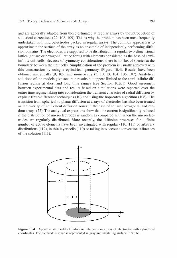
and are generally adapted from those estimated at regular arrays by the introduction ofstatistical corrections (22, 108, 109). This is why the problem has been most frequentlyundertaken with microelectrodes packed in regular arrays. The common approach is toapproximate the surface of the array as an ensemble of independently performing diffu-sion domains. The electrodes are supposed to be distributed in a regular two-dimensionallattice (square or hexagonal lattice form) with elements considered as the base of semi-infinite unit cells. Because of symmetry considerations, there is no flux of species at theboundary between the unit cells. Simplification of the problem is usually achieved withthis construction by using a cylindrical geometry (Figure 10.4). Results have beenobtained analytically (9, 105) and numerically (3, 10, 13, 104, 106, 107). Analyticalsolutions of the models give accurate results but appear limited to the semi-infinite dif-fusion regime at short and long time ranges (see Section 10.5.1). Good agreementbetween experimental data and results based on simulations were reported over theentire time regime taking into consideration the transient character of radial diffusion byexplicit finite-difference techniques (10) and using the hopscotch algorithm (106). Thetransition from spherical to planar diffusion at arrays of electrodes has also been treatedas the overlap of equivalent diffusion zones in the case of square, hexagonal, and ran-dom arrays (22). The analytical expressions show that the current is significantly reducedif the distribution of microelectrodes is random as compared with when the microelec-trodes are regularly distributed. More recently, the diffusion processes for a finite number of active elements have been investigated with regular (110, 111) or arbitrarydistributions (112), in thin layer cells (110) or taking into account convection influencesof the solution (111).
10.3 Theory: Diffusion at Microelectrode Arrays 399
Figure 10.4 Approximate model of individual elements in arrays of electrodes with cylindricalcoordinates. The electrode surface is represented in gray and insulating surface in white.
Ch010.qxd 10/20/2006 3:37 PM Page 399
10.3.2 Arrays of electrodes operating in generator/collector mode
The intrinsic difficulties of modeling diffusion at arrays of electrodes are increased in thegenerator/collector mode because the transport equations must be solved numerically ratherthan analytically. The discontinuities between electrodes and insulators are amplified as thetwo adjacent electrodes interact with each other leading to cross talk at their immediate bor-ders. Moreover, the communication between each electrode involves long-distance diffu-sional pathways, which connect the electrodes by their opposite borders. As a consequence,all numerical techniques have to deal with fine space grids between the electrodes todescribe precisely the diffusion pathways at distances exceeding the electrode dimensions.The problem must be solved simultaneously at two different scales depending on the dis-tance z from the array surface. For these reasons, simulations performed in real space areextremely difficult to handle as they require grid spaces perfectly adapted to the problemunder investigation with a large number of points or nodes to be treated together. In aneffort to reduce the number of grid elements required, simulations at electrodes arrays haveemployed exponential space grids (54, 74) or particular grid discretization (77) with theadvantage of producing a high grid density in the vicinity of the electrodes without a dra-matic increase in the overall number of elements required for the simulation of the com-plete diffusion layer. However, one major disadvantage is that the grid lines do not followthe actual lines of flux to the electrode surface especially at the edges of the electrodeswhere they are strongly curved. Moreover, it is impossible to define precisely a single gridaccounting for the time-dependent shape of the concentration profiles.
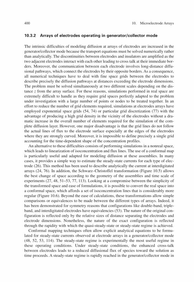
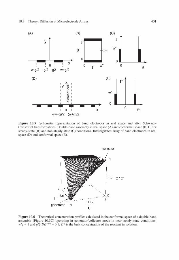
An alternative to these difficulties consists of performing simulations in a nonreal space,which leads to linearization of isoconcentration and flux lines. The use of a conformal mapis particularly useful and adapted for modeling diffusion at these assemblies. In manycases, it provides a simple way to estimate the steady-state currents for each type of elec-trode (26). This method has been used to describe analytically the current at interdigitatedarrays (24, 76). In addition, the Schwarz–Christoffel transformation (Figure 10.5) allowsthe best change of space according to the geometry of the assemblies and time scale ofexperiments (27, 48, 51–53, 77, 113). Looking at a compromise between the simplicity ofthe transformed space and ease of formulations, it is possible to convert the real space intoa conformal space, which affords a set of isoconcentration lines that is considerably moreregular (Figure 10.6). Beyond the ease of calculations, these transformations allow simplecomparisons or equivalences to be made between the different types of arrays. Indeed, ithas been demonstrated for symmetry reasons that configurations like double-band, triple-band, and interdigitated electrodes have equivalencies (53). The nature of the original con-figuration is reflected only by the relative sizes of distance separating the electrodes andelectrode dimensions. Nonetheless, the nature of the exact configuration is reflectedthrough the rapidity with which the quasi-steady-state or steady-state regime is achieved.
Conformal mapping techniques often allow explicit analytical equations to be formu-lated for steady-state currents observed at electrode arrays in a generator/collector mode(48, 52, 53, 114). The steady-state regime is experimentally the most useful regime inthese operating conditions. Under steady-state conditions, the enhanced cross-talkbetween electrodes leads to a reduced diffusional flux of species toward the solution astime proceeds. A steady-state regime is rapidly reached in the generator/collector mode in
400 10. Microelectrode Arrays
Ch010.qxd 10/20/2006 3:37 PM Page 400
10.3 Theory: Diffusion at Microelectrode Arrays 401
Figure 10.5 Schematic representation of band electrodes in real space and after Schwarz–Christoffel transformations. Double-band assembly in real space (A) and conformal space (B, C) forsteady-state (B) and non-steady-state (C) conditions. Interdigitated array of band electrodes in realspace (D) and conformal space (E).
Figure 10.6 Theoretical concentration profiles calculated in the conformal space of a double-bandassembly (Figure 10.3C) operating in generator/collector mode in near-steady-state conditions.w/g = 1 and g/2(Dt)�1/2 = 0.1. C* is the bulk concentration of the reactant in solution.
Ch010.qxd 10/20/2006 3:37 PM Page 401
contrast to arrays of electrodes operating at the same potential. The greater the feedbackand collection efficiency between the electrodes, the more rapid is the approach to thesteady state. The conformal space also allows effective numerical simulations to be per-formed under non-steady-state conditions whenever planar diffusion is significantlyaltered by nonplanar diffusion. Under non-steady-state conditions, the grid lines do notnecessarily follow those of the conformal map, but the map is advantageous over otherconfigurations as it more closely approximates the actual grid. A smaller number of nodesare necessary to obtain a numerical solution with the accuracy required. These conformaltechniques also allow the effect of electrode perturbation on the electrochemical responseto be evaluated for simple geometries. It has been demonstrated for double-hemicylindricalelectrodes that these effects are no longer negligible when the resulting heights of the elec-trodes from the insulating plane become comparable to their widths or to the distance sep-arating the electrodes (114).
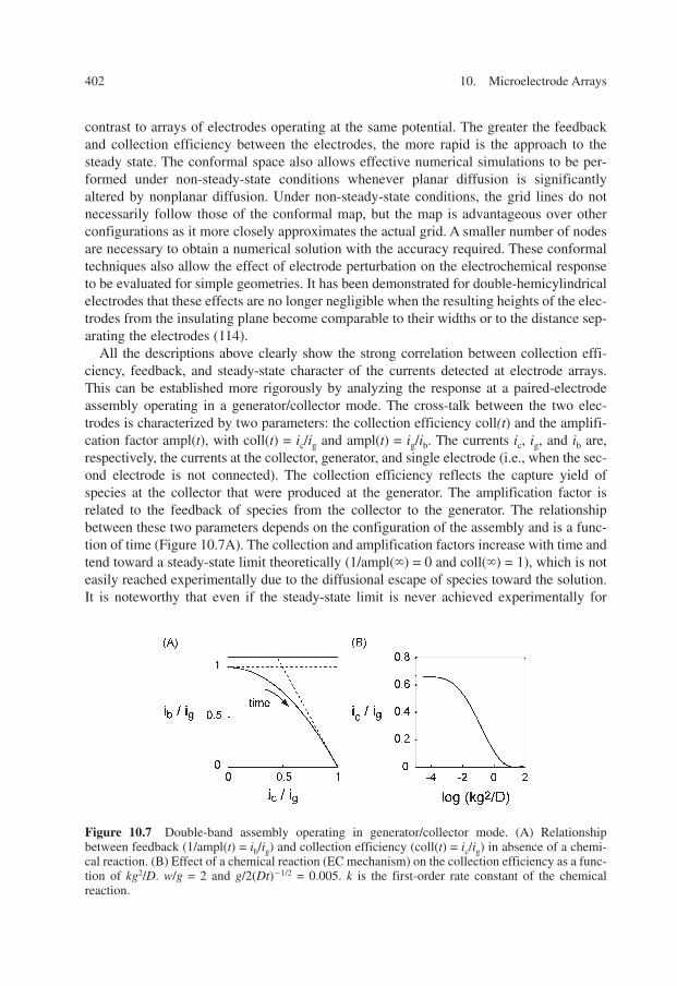
All the descriptions above clearly show the strong correlation between collection effi-ciency, feedback, and steady-state character of the currents detected at electrode arrays.This can be established more rigorously by analyzing the response at a paired-electrodeassembly operating in a generator/collector mode. The cross-talk between the two elec-trodes is characterized by two parameters: the collection efficiency coll(t) and the amplifi-cation factor ampl(t), with coll(t) = ic/ig and ampl(t) = ig/ib. The currents ic, ig, and ib are,respectively, the currents at the collector, generator, and single electrode (i.e., when the sec-ond electrode is not connected). The collection efficiency reflects the capture yield ofspecies at the collector that were produced at the generator. The amplification factor isrelated to the feedback of species from the collector to the generator. The relationshipbetween these two parameters depends on the configuration of the assembly and is a func-tion of time (Figure 10.7A). The collection and amplification factors increase with time andtend toward a steady-state limit theoretically (1/ampl(�) = 0 and coll(�) = 1), which is noteasily reached experimentally due to the diffusional escape of species toward the solution.It is noteworthy that even if the steady-state limit is never achieved experimentally for
402 10. Microelectrode Arrays
Figure 10.7 Double-band assembly operating in generator/collector mode. (A) Relationshipbetween feedback (1/ampl(t) = ib/ig) and collection efficiency (coll(t) = ic/ig) in absence of a chemi-cal reaction. (B) Effect of a chemical reaction (EC mechanism) on the collection efficiency as a func-tion of kg2/D. w/g = 2 and g/2(Dt)�1/2 = 0.005. k is the first-order rate constant of the chemicalreaction.
Ch010.qxd 10/20/2006 3:37 PM Page 402
micrometric arrays, an intermediate regime is attained. In these conditions, a simple rela-tion exists between coll(t) and ampl(t):
(10.4)
with � = 0.5 for a double-band assembly (113), � = 0.25 for a triple-band configuration(one generator flanked by two collectors) (31) and even smaller for an interdigitated array.The � value accounts for the extent of diffusional escape toward the solution according to the configuration of the assembly. It thus reflects the time dependence or rapidity inwhich the steady-state regime is achieved. Indeed, this regime is approached faster for aninterdigitated array whereas it remains a virtual limit for a double-band configuration ofmicrometric size.
The collection efficiency is related to the geometry of the assembly itself but dependsalso on the lifetime of species produced at the generator. Indeed, one of the main interestsof these assemblies is their capability to address kinetic problems. When this lifetimeexceeds the time required to diffuse between the two electrodes, the collection efficiency isthus maximal according to the configuration of the assembly. In contrast, when the gener-ated species is no longer stable, the collection efficiency tends to be zero. In this case, thetemporal notion is replaced by a spatial notion linked to the dynamics of diffusion takingplace between the electrodes. This is true whatever the geometry of the assembly providedthat the duration of the experiment is sufficiently long for the diffusion layer developing atthe generator to extend over the collector. The collection efficiency is thus a function thatcompares the relative values of lifetime with the time of flight over the distance separatingthe two electrodes (Figure 10.7B). Under these conditions, experimental determinations ofrate constants or electrochemical mechanism need preliminary working curves to be estab-lished with respect to the configuration and geometry of the device (27, 53). This remainsvalid even if the generator/collector mode is employed in an electroanalytical approach fordiffusion layer titrations in which the reactant is produced at the generator and reacts withthe target analyte. As the collection efficiency is very sensitive to the heterogeneous kinet-ics of electron transfer at the generator (49), the need for analytical measurements to pro-ceed with quantitative simulation appears to be obvious. Moreover, the array and especiallythe distance between the generator and collector must be adapted to the kinetics underinvestigation. Indeed, for the majority of molecules, the diffusion coefficient is equal to D � 10�5 cm2 sec�1, which means that a lifetime of 1 ms requires formally a interelectrodedistance of about 1 �m (Figure 10.7B).
10.4 FABRICATION OF MICROELECTRODE ARRAYS
Numerous methods for fabricating microelectrode arrays have been devised depending onthe type of array required (6, 20, 35, 41, 49, 62, 63, 65, 115–134).
Low-aspect-ratio (ratio of the height of the microelectrode divided by its lateral dimensionis larger than 0.2) microelectrode arrays are fabricated using conventional silicon-basedmicrofabrication technologies, such as lithographic techniques to yield arrays of thin filmsof metallic or carbon electrodes on a silicon substrate. These arrays often have limited sta-bility and life times as a result of defects in the metal layer; poor resistance to corrosion is
coll ampl( ) / ( )t t= 1− �
10.4 Fabrication of Microelectrode Arrays 403
Ch010.qxd 10/20/2006 3:37 PM Page 403
observed together with subsequent swelling and delamination of the metal layers. Thesemicrofabricated arrays are typically fragile and cannot be cleaned using conventional clean-ing methods, for example, polishing, washing with solvents, and sonication. They are mostlycleaned using reactive ion etching with oxygen plasma.
High-aspect-ratio (ratio of the height of the microelectrode divided by its lateraldimension is larger than 2) microelectrode arrays are mostly fabricated using siliconmicromachining, silicon microfabrication, or techniques involving bundling of multiplemetal wires. These arrays are mostly designed to penetrate brain tissue to permit highlylocalized electrical stimulation and/or recording signals from neural tissue. These arraysare more robust compared with arrays formed by lithography and the surface is rathereasy to clean. However, solid wire electrode arrays do not have more than a handful ofelectrodes in the array. The Utah Electrode Array contains about 100 electrodes but is lessprone to delamination.
10.4.1 Mechanical methods
A variety of methods have been used in fabricating microdisk electrodes (see Chapter 9).One of the most successful methods is that in which a wire is sealed in glass and the sur-face is subsequently polished (or etched away) until the electrode is revealed (135). Themanufacturing of microdisk arrays is based on the same technique as for simple electrodes.Although lithographic methods or silicon technology are the preferred ways in industry forthe mass fabrication of ordered arrays, these techniques are not always accessible to mostanalytical users of microelectrodes. There is thus demand for the availability of inexpen-sive, conventionally manufactured microelectrodes. These processes, which are mostlymechanical methods, are at present limited due to the poor reproducibility of the manu-facturing methods. Mechanical methods, summarized in Figure 10.8, can be classifiedaccording to how the array is constructed. A major limitation is that a careful polishingtechnique has to be employed. Otherwise, the electrodes have a tendency to recess belowthe surface of the insulating sheet leading to voltammograms that are slightly differentfrom those for a perfectly coplanar electrode. Careful design is essential to ensure that thediffusion layers at each microelectrode do not interfere with others.
10.4.1.1 Wire techniques
One of the current technologies involves sealing conducting wires (gold, platinum, andcarbon fibers) into an insulating material (epoxy resin and glass tube), which is resistantto water and some organic solvents, such as acetonitrile and methanol (Figure 10.8A) (29,65, 90, 117, 137). Electrical contact between the metal wires is made by using silver epoxyresin. This method was used by Schwarz et al. (137), in developing microelectrode arraysof gold and platinum with different numbers of single electrodes in the array. They showedthat the construction of disk as well as band microelectrode arrays is possible using thismechanical method. The ordered arrays were constructed by clamping the metal wires onan H-shaped body made of bronze. The wires are fixed in notches with fixed internal dis-tance of 120–130 �m between the single wires. Then the wires are put into a mould and
404 10. Microelectrode Arrays
Ch010.qxd 10/20/2006 3:37 PM Page 404
epoxy resin is poured in to give a cube-shaped epoxy resin body. Arrays of disks as wellas band electrodes were constructed in this way.
Band electrodes were formed by pressing gold foils with resin-impregnated glass silkfabric, as the insulation layer, at temperatures of 120–150 �C (137). The distance betweenthe bands is 120 �m and the length of the bands is 600 �m with 2 mm width. The elec-trodes are provided with an electrical connector at the end of the contact cap. The radii ofthe sensor surfaces are 2 mm, with complete lengths of 25 mm.
Carbon fibers have been used for array construction because they are more rigid thangold. The construction of carbon fiber arrays consisting of five layers of 20 electrodes wasintroduced by Caudill et al. (29) and used as a flow rate independent amperometric detec-tor. Sleszynski et al. (25) reported the design of ensembles based on reticulate vitreouscarbon embedded in epoxy resin.
10.4.1.2 Sandwich method
Sandwich techniques (Figure 10.8B) are ideal for the construction of double-bandassemblies (53, 113). The schematic of a double-band electrode is seen in Figure 10.1C.An insulator (Mylar film of 2.5 �m thickness, insulating gap) is placed between twosheets of platinum foil (5 �m) and the entire assembly inserted between two pieces ofsoft glass (about 3 mm thick and 8 mm width). Each layer of this sandwich is sealed witha small amount of epoxy resin, before firmly pressing into position. After hardening ofthe epoxy, each platinum foil was independently connected to an electrical copper leadwith silver epoxy. This assembly can be glued into a glass tube (1 cm internal diameter).
10.4 Fabrication of Microelectrode Arrays 405
Figure 10.8 Construction principles of microelectrode arrays: (A) wire technique, (B) sandwichmethod, (C) composite formation (reprint with permission from reference (15)), and (D) Sono-chemical formation, electrical micrograph with permission from reference (136).
Ch010.qxd 10/20/2006 3:37 PM Page 405
The cross-section of this assembly can be exposed by saw yielding an assembly of two-paired microband electrodes.
An inexpensive and general method for the construction of microelectrode arrays isbased upon thermal lamination of metal foils, which is very similar to the sandwich tech-nique described before (138). The polyester/polyethylene laminating foil used is resistantto DMSO as well as to DMF. Electrical connections to the foil have been established eitherby spot welding a thin metal wire contact to the foil or by using a piece of copper foil witha conducting adhesive on one side. Gold, platinum, and silver microbands were fabricatedin this way in addition to disks ranging from 10 to 125 �m. A linear array of microdiskelectrodes was prepared by laminating two gold meshes (Figure 10.8E).
10.4.1.3 Formation of compositions (composite electrodes)
Ke�I graphite electrodes are composite electrodes with islands of graphite particles in asea of Ke�I (13). Each island of graphite is in effect a microelectrode, each separated fromother microelectrodes by insulating regions of Ke�F. The electrode surface is thus consid-ered to consist of an array of microelectrodes (Figure 10.8C). It can be considered as a par-tially blocked solid carbon electrode. The electrode can be fabricated by mixing graphite(particle size of less than 1 �m) with Ke�F (150–450 �m particle size) with a mortar andpestle. This mixture was put into a vacuum chamber to remove the air from the compos-ite and heated to 300–325 �C for 5 min. As the pressure increased, the heater turned offresulting in the composite pellet, which was mounted on a glass tube and sealed in placewith epoxy. The dimensions of active and inactive sites on the electrode surface can beadjusted by varying the Ke�I particle size and carbon content. The graphite particles incor-porated in an inert binder were found to exhibit microelectrode character in the range of5–25% graphite. These electrodes are widely used as oxidative working electrodes in flow-ing streams because of their favorable noise and detection limit.
Another composite electrode is constructed by filling the voids of reticulated vitreouscarbon with nonconductive epoxy to produce two-dimensional electrode materials (25).Reticulated vitreous carbon has been used as a three-dimensional highly porous electrodematerial and has been used in flowing systems as well as in thin slices as an optically trans-parent electrode.
Electrodes constructed of a single piece of material, such as reticulated vitreous carbon,have the advantage of good electrical contact to each conducting surface, but possess theattendant disadvantage that the magnitude of the interdistance spacing between the elec-trodes is limited by the requirement that the material be dimensionally stable. Microcellularfoams made out of carbonized poly(acrylonitrile) (PAN) foams have been shown to beadvantageous as the interelectrode spacing increases as the void fraction of the foam alsoincreases. These foams are prepared via a thermally induced phase separation that allowscontrol of density, pore size, and large void volume (97%). By incorporating an insulatorinto this matrix, an array can be made of average conducting particle size of 1 �m andsmaller (139). Cylindrical samples of PAN foams were fashioned by using a simple drillpress. The drill was suspended over a lab jack where the sample was placed. As the jackwas raised, the drill slowly turned cutting the fragile foam structure. Filling of the foamwith epoxy was accomplished in a vacuum through capillary action.
406 10. Microelectrode Arrays
Ch010.qxd 10/20/2006 3:37 PM Page 406
10.4.1.4 Sonochemical fabrication
Arrays can also be fabricated by sonochemical ablation of polydiamidobenzene ultra thinfilms deposited on gold-coated glass slides (136). These electrodes were then immersed ina beaker containing distilled water and sonicated for an hour using a 25-kHz sonic bath.The sonic bath employed 12 transducers geometrically arranged and bonded to the base ofthe stainless steel tank. 1,2-Diaminobenzene dihydrochloride can be electropolymerized atconductive surfaces via a two-electron process to form essentially defect-free insulationpolymer films of less than 100 nm thickness. The rational underpinning of this work is thatsonochemical ablation of thin insulation polymer films at electrode surfaces may exposelocalized areas each of which can act as localized microelectrodes and collectively as amicroelectrode array. Ultrasound in the kHz range passing through solvents, such as watercauses thermal agitation and localized hotspots of up to several hundreds to a few thou-sand K. This in turn gives rise to the formation of superheated vapor bubbles, which arecooled by the solvent at ambient temperature and asymmetrically implode with the ejec-tion of micro-jets of solvents at speeds of up to several hundreds msec�1. This micro-jetcan cause the shattering of hard brittle solids. Soft polymer may, however, be ablated bysuch jets. A SEM image for a 60-sec sonicated electrode assembly is shown in Figure 10.8Dshowing the cavitations of the polymer surface. The size of the cavities are about 3 � 1 �mor sub-micron diameter.
10.4.2 Template approaches
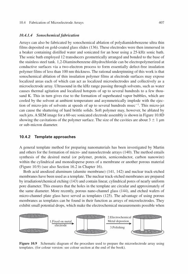
A general template method for preparing nanomaterials has been investigated by Martinand others for the formation of micro- and nanoelectrode arrays (140). The method entailssynthesis of the desired metal (or polymer, protein, semiconductor, carbon nanowire)within the cylindrical and monodisperse pores of a membrane or another porous material(Figure 10.9) (see also Section 16.2 in Chapter 16).
Both acid anodized aluminum (alumite membrane) (141, 142) and nuclear track-etchedmembranes have been used as a template. The nuclear track-etched membranes are preparedby irradiation/chemical etching (143) and contain linear, cylindrical pores of nearly uniformpore diameter. This ensures that the holes in the template are circular and approximately ofthe same diameter. More recently, porous nano-channel glass (144), and etched wafers ofmicro-channel plate glass have served as templates (125). The advantage of using porousmembranes as templates can be found in their function as arrays of microelectrodes. Theyexhibit small potential drops, which make the electrochemical measurements possible when
10.4 Fabrication of Microelectrode Arrays 407
2.ElectrochemicalMetal depostion
3.Polishing
1.Fixed on metalelectrode
Figure 10.9 Schematic diagram of the procedure used to prepare the microelectrode array usingtemplates. (for colour version: see colour section at the end of the book).
Ch010.qxd 10/20/2006 3:37 PM Page 407
a low-concentration electrolyte is used. Furthermore, membranes with pore radii rangingfrom 6 �m to 50 Å and pore densities, ranging from 1 � 105 pores cm�2 to about 6 � 108
are commercially available allowing the formation of arrays with a broad range of elementradii. The ability to control the length of the electrodes formed in the template is anotherimportant feature of the template method. The length of the wire can be controlled by vary-ing the deposition time (electrochemical plating method) or by varying the thickness of thetemplate in the electroless plating approach. The template technique is so advanced that goldmetal wires as small as 80 Å in diameter can be produced (142).
The fabrication of these arrays presents three challenges:
(1) Preparation of the porous template(2) Electrodeposition of the metal within the hollow parts of the template(3) Final preparation of the array following electrodeposition
One of the earliest applications of the template method was to prepare ensemble micro-scopic (7, 18) and nanoscopic electrodes (116, 141). Such electrodes were prepared byelectrochemically depositing noble metals within the pores of the commercially availablepolymeric filtration membranes. The fabrication of a microelectrode “ensemble” based onthe electrochemical deposition of platinum into the pores of a track-etched microporouspolycarbonate host membrane was first shown in 1987 by Charles Martin (7). The wordensemble was used to describe the final device because the elements in the device are notevenly spaced. The procedure is simple, and requires only routine and inexpensive elec-trochemical instrumentation. It was ultimately found that electroless plating allowed formore uniform metal deposition (116). Both plating methods are important for the fabrica-tion of the array, and further considerations continue in the following.
10.4.2.1 Electrochemical plating method
Electrodeposition of metallic wires throughout the void spaces of porous nanostructuretemplates was first shown by Possin in 1970 (145), who developed an electrochemicalsynthesis method for producing different single metal wires in a 15-�m thick mica waferwith the density of the pores in the order of 104 pores cm�2. As the membranes employedhave cylindrical pores of uniform diameter a micro- as well as nanometer-sized cylinderor fibril of the desired material is obtained in each pore (7, 146–150).
To electrodeposit metal throughout the channels of the template, the porous materialis mounted on a metal-coated glass substance; typically, a metal-coated glass slide(Figure 10.9). The slide provides support for the template and the metal coating on theslide provides the electrical connection needed to drive the electrodeposition. The tem-plates are often coated on one side with a thin metal layer (100 nm of titanium, platinum,or gold) through sputtering in the vacuum at an angle of 45� with respect to the plane ofthe wafer. This allows the metal to deposit uniformly on the edges of the template as wellas a short distance into the channels. These metalized templates adhere well to the glassand provide a surface from which the electrodeposited metal can grow. Ideally, the metalfilm should completely occlude the channel ends, providing a continuous conducting sur-face in the channels. Large channels (�1 �m) cannot be efficiently occluded by sputtering
408 10. Microelectrode Arrays
Ch010.qxd 10/20/2006 3:37 PM Page 408
layers of metal from which wire growth can be initiated. The template can be bound to themetal-coated slide using epoxy applied around the periphery: a light downward forceapplied to the center of the template during the epoxy step followed by curing to ensurethat the template maintains good electrical contact. Electrodeposition is often enhanced atelevated temperatures and the solutions are often chemically harsh. Thus, a hard, inertepoxy is needed to withstand harsh conditions. Electrodeposition of gold, platinum, silver,copper, nickel, rhodium, and cobalt in templates has been reported (7, 125, 141, 142, 145,150–152) as well as deposition of polymer (149), semiconductors (153), and carbon (154)into these templates.
10.4.2.2 Electroless metal deposition
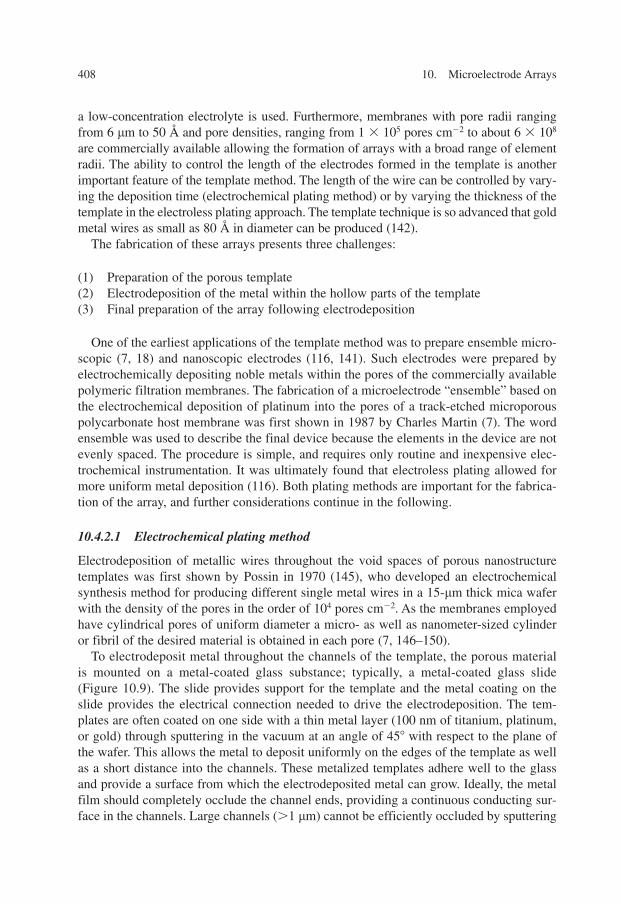
Electroless deposition of metals is based on the deposition and reduction of metallic ions(reducing agents are formaldehyde, hydrazine, hydroxylamine) (155–158) from a solutionto a surface without applying an electrical potential (159). The key feature of the electro-less deposition process is that gold deposition begins at the pore wall. The advantage ofthe electroless method is that the surface to be coated does not need to be electrochemi-cally conductive. The key requirement of an electroless deposition bath of this type is toarrange the chemistry such that the kinetics of homogeneous electron transfer from thereducing agent to the metal ion is slow. This is essential because otherwise the metal ionwould simply be reduced in the bulk solution. A catalyst that accelerates the rate of metal-ion reduction is thus applied to the surface to be coated. In this way, metal ions are reducedonly at the surface and the surface becomes coated with the desired metal.
Electroless deposition of various metals into templates was pioneered by Martin whoalso showed that more uniform metal films are obtained as thicker metal layers are formed(116). Furthermore, the electroless deposition chemistry allows routine fabrication of golddisk electrode arrays, in which the disk can have a diameter as small as 10 nm. To makethe electroless deposition process compatible with the membrane chemistry, a “sensitizer”(Sn2+) was first applied to the surface of the membrane, by simply immersing the mem-brane in a solution of SnCl2/trifluoroacetic acid (0.026/0.07 M) (Figure 10.10).
10.4 Fabrication of Microelectrode Arrays 409
Si
Si
OH
Si
OH
OH
O
Si
SiO
Si
O
O
Sn2+Sn2+
Sn2+
Si OH SiAgNO3
OSi
Si
O
SiOO
Sn4+
Sn4+
Si
Ag(surface)
2 Au+H H
O3OH-
+ H-
O+ 2 H2O
O
Si
Si
O
Si
O
O
Sn4+
Sn4+
Si
+ Ag(surface)
+
OSi
Si
O
SiOO
Sn4+
Sn4+
Si
+ Au(surface)+ +O
Figure 10.10 Schematic diagram of the electroless procedure used to deposit gold into templates.
Ch010.qxd 10/20/2006 3:37 PM Page 409
The Sn2+ sensitized polycarbonate membrane is then activated by immersion in anaqueous solution of AgNO3 for some minutes. This causes a redox reaction in which thesurface-bound Sn2+ is oxidized to Sn4+ and the Ag+ is reduced to elemental Ag togetherwith some silver oxide. As a result, the pore walls become coated with discrete nanoscopicAg particles. A gold-coated membrane can be obtained by immersing it into a Au platingbath (Na3Au(SO3)2) (commercially available from Technic Inc., Craston, RI: OROMERSESO Part B) in the presence of formaldehyde and Na2SO3. The Ag particles are galvanicallydisplaced by gold as gold is the more noble material. Furthermore, the silver particlesshow excellent catalytic sites for the oxidation of formaldehyde:
(10.5)
(10.6)
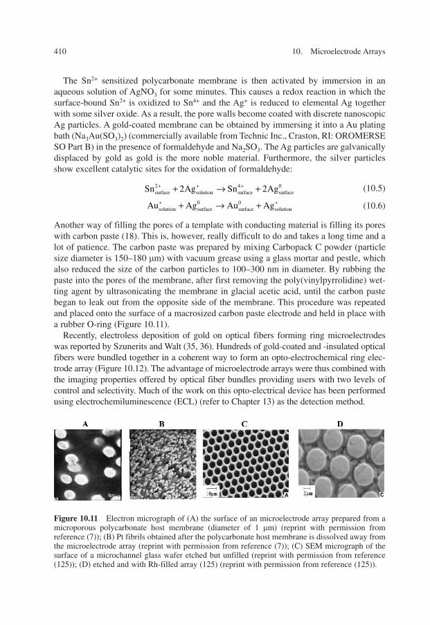
Another way of filling the pores of a template with conducting material is filling its poreswith carbon paste (18). This is, however, really difficult to do and takes a long time and alot of patience. The carbon paste was prepared by mixing Carbopack C powder (particlesize diameter is 150–180 �m) with vacuum grease using a glass mortar and pestle, whichalso reduced the size of the carbon particles to 100–300 nm in diameter. By rubbing thepaste into the pores of the membrane, after first removing the poly(vinylpyrrolidine) wet-ting agent by ultrasonicating the membrane in glacial acetic acid, until the carbon pastebegan to leak out from the opposite side of the membrane. This procedure was repeatedand placed onto the surface of a macrosized carbon paste electrode and held in place witha rubber O-ring (Figure 10.11).
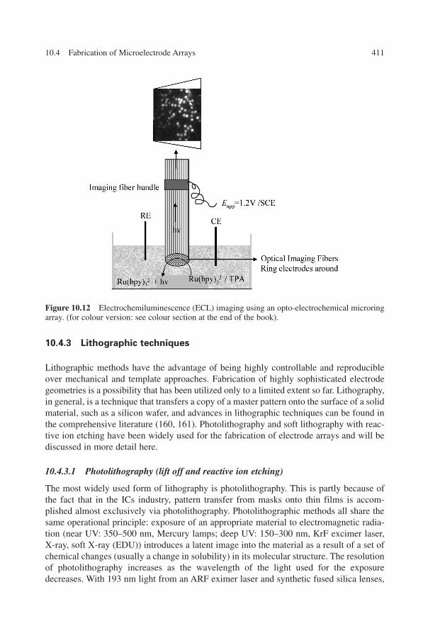
Recently, electroless deposition of gold on optical fibers forming ring microelectrodeswas reported by Szunerits and Walt (35, 36). Hundreds of gold-coated and -insulated opticalfibers were bundled together in a coherent way to form an opto-electrochemical ring elec-trode array (Figure 10.12). The advantage of microelectrode arrays were thus combined withthe imaging properties offered by optical fiber bundles providing users with two levels ofcontrol and selectivity. Much of the work on this opto-electrical device has been performedusing electrochemiluminescence (ECL) (refer to Chapter 13) as the detection method.
Au Ag Au Agsolution surface0
surface0
solution+ ++ +→
Sn Ag Sn Agsurface2
solution surface4
surface0+ + ++ → +2 2
410 10. Microelectrode Arrays
Figure 10.11 Electron micrograph of (A) the surface of an microelectrode array prepared from amicroporous polycarbonate host membrane (diameter of 1 �m) (reprint with permission from reference (7)); (B) Pt fibrils obtained after the polycarbonate host membrane is dissolved away fromthe microelectrode array (reprint with permission from reference (7)); (C) SEM micrograph of thesurface of a microchannel glass wafer etched but unfilled (reprint with permission from reference(125)); (D) etched and with Rh-filled array (125) (reprint with permission from reference (125)).
Ch010.qxd 10/20/2006 3:37 PM Page 410
10.4.3 Lithographic techniques
Lithographic methods have the advantage of being highly controllable and reproducibleover mechanical and template approaches. Fabrication of highly sophisticated electrodegeometries is a possibility that has been utilized only to a limited extent so far. Lithography,in general, is a technique that transfers a copy of a master pattern onto the surface of a solidmaterial, such as a silicon wafer, and advances in lithographic techniques can be found inthe comprehensive literature (160, 161). Photolithography and soft lithography with reac-tive ion etching have been widely used for the fabrication of electrode arrays and will bediscussed in more detail here.
10.4.3.1 Photolithography (lift off and reactive ion etching)
The most widely used form of lithography is photolithography. This is partly because ofthe fact that in the ICs industry, pattern transfer from masks onto thin films is accom-plished almost exclusively via photolithography. Photolithographic methods all share thesame operational principle: exposure of an appropriate material to electromagnetic radia-tion (near UV: 350–500 nm, Mercury lamps; deep UV: 150–300 nm, KrF excimer laser,X-ray, soft X-ray (EDU)) introduces a latent image into the material as a result of a set ofchemical changes (usually a change in solubility) in its molecular structure. The resolutionof photolithography increases as the wavelength of the light used for the exposuredecreases. With 193 nm light from an ARF eximer laser and synthetic fused silica lenses,
10.4 Fabrication of Microelectrode Arrays 411
Figure 10.12 Electrochemiluminescence (ECL) imaging using an opto-electrochemical microringarray. (for colour version: see colour section at the end of the book).
Ch010.qxd 10/20/2006 3:37 PM Page 411
patterns as small as 150 nm are achieved (162). However, it has been pointed out that pho-tolithographically produced electrodes are difficult to resurface by means of polishing(163). One should keep in mind that the procedure of polishing electrodes between meas-urements is out of the question when it comes to practical applications, such as processmonitoring or in situ investigations.
Three steps are important for the success of photolithography and for forming micro-electrode arrays:
(1) Photo mask design(2) Photoresist step(3) Development
(a) Photo mask designAlthough a scanned aperture can be used to write arbitrary patterns, the predominant useof photolithography is in replicating a pattern on a mask into a layer of photoresist. Sucha mask, also called photo mask, is either a nearly optical flat glass, which is transparent tonear UV or a quartz plate, transparent to deep UV covered with a metal absorber pattern(about 800 Å thick chromium layer). Such a mask is either placed in physical contact withthe resists (contact mode), or an image of the mask is reduced and projected into the resistswith an optical system (projection mode).
(b) Photoresist stepIn addition to advances in the physics and engineering of new light sources and projectionoptics, clear designs for the chemistries of the photoresist have been critical to the successof photolithography. Photoresists must meet several rigorous requirements: high sensitivity,high contrast, good etching resistance, good resolution, easy processing, high purity, min-imal solvent use, low cost, and a high glass transition temperature, Tg. Most resists areamorphous polymers. At temperatures above the glass transition temperature, these poly-mers exhibit viscous flow with motion of the polymer chain segments. At a temperaturebelow Tg, the motion of the segments is halted and the polymer behaves as a glass ratherthan as a rubber. Thus, heating the resists film above the Tg enables the film to anneal intoits most stable energetic state, the rubber state. Here, the solvent easily can be removedfrom the polymer matrix through soft-bake. The photoresist is dispensed from a vicioussolution of the polymer into the wafer laying on a wafer plate in a resist spinner.
The principle components of photoresists are a polymer, a sensitizer, and a casting sol-vent. During radiation, the polymer changes structure. The solvent allows spin coating andthin layer formation on a wafer surface. Sensitizers control the chemical reactions in thepolymeric phase. There are two types of resists: positive and negative resists. We talkabout a positive resist when the photochemical reaction during exposure weakens the poly-mer by rupture or scission of the main and side polymer chains. The exposed resistsbecome more soluble in developing solutions. The development rate for the exposed resistis larger than for the unexposed one. A negative resist is where the reaction strengthens thepolymer by random cross-linking, thus, becoming less soluble. The best known positivephotoresist is poly(methylmethacryalte) (PMMA). PMMA becomes soluble through chainscission under deep UV illumination with the maximal sensitivity at 220 nm. Negativephotoresists are mostly based on cross-linking of polymer chains, rendering the exposed
412 10. Microelectrode Arrays
Ch010.qxd 10/20/2006 3:37 PM Page 412
parts of the resist insoluble. One negative resist commonly used is a bis(aryl)azide rubberresist, whose matrix is cyclized poly(cis-isoprene). Upon photolysis, this resist loses nitro-gen and generates a highly reactive nitrene, which undergoes a series of reactions thatresult in the cross-linking of the resin. New types of resists include polyimides, polyamicacids, photosensitive polyimide precursors, SU-8 (an epoxy-based transparent photore-sist). All the resists are deposited through spin coating, which is of primary importance tothe effectiveness of pattern transfer.
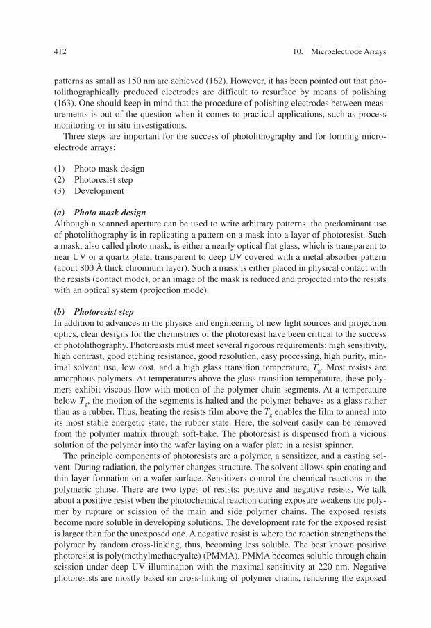
(c) DevelopmentThe development of the resin to form microelectrode arrays is mostly based on the “lift-offprocess” (164). A solvent dissolves the remaining soluble positive photoresist underneaththe metal, starting at the edge or lip of the unexposed photoresist and lift off the metal inthe process (Figure 10.13). When the photoresist is removed, all metal on top of the pho-toresist strip strips off automatically while metal on the top of the photoresist lines stays.
Photolithographically patterned gold microelectrodes have been used extensively (165).Pishko et al. reported recently the fabrication of glucose, lactate, and pyruvate sensorarrays by depositing electrostatically complexed monolayers on lithographically patternedindividually addressable, gold microelectrodes. Standard photolithographic techniquescombined with metal deposition were used to fabricate gold arrays of both SiO2/Si andflexible Mylar substrates.
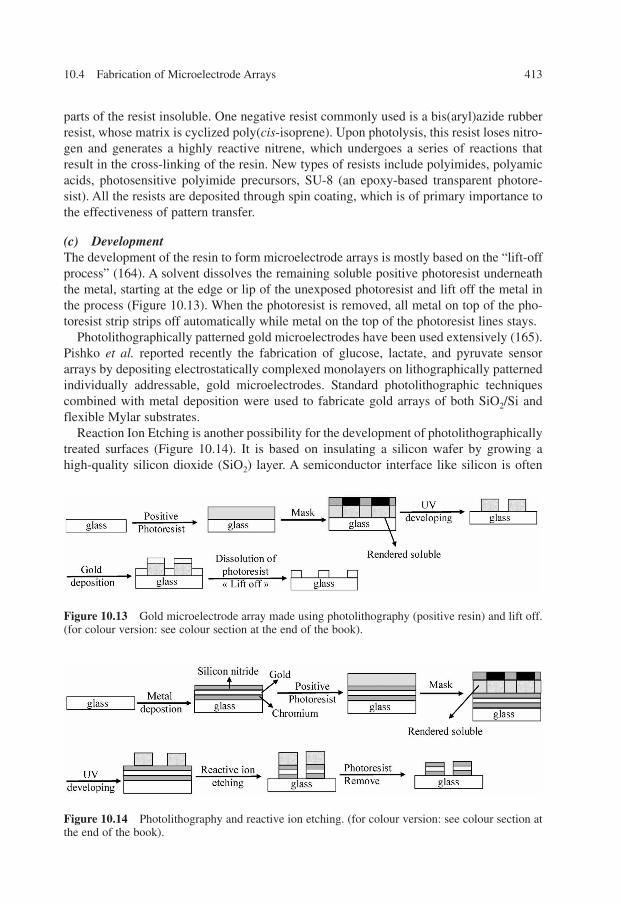
Reaction Ion Etching is another possibility for the development of photolithographicallytreated surfaces (Figure 10.14). It is based on insulating a silicon wafer by growing a high-quality silicon dioxide (SiO2) layer. A semiconductor interface like silicon is often
10.4 Fabrication of Microelectrode Arrays 413
Figure 10.14 Photolithography and reactive ion etching. (for colour version: see colour section atthe end of the book).
Figure 10.13 Gold microelectrode array made using photolithography (positive resin) and lift off.(for colour version: see colour section at the end of the book).
Ch010.qxd 10/20/2006 3:37 PM Page 413
preferred over glass as it is perfectly flat and withstands the subsequent processing steps.Onto the SiO2, a thin metal film (10–100 nm) is deposited followed by deposition of aninsulating film, Si3N4, on top of the metal using plasma chemical vapor deposition (CVD).This multilayer surface is modified with a photoresist, covered with a photomask, exposedto UV light, and developed. The area, which is not protected with resin, is exposed to reac-tive ion etching to etch away the top insulator and the metal. The advantage of reactive ionetching is that the patterns have extremely sharp and vertical steps.
10.4.3.2 Other lithographic techniques (X-ray, electron-beam, ion-beam)
The improvement in optical resolution can be achieved either by increasing the numericalaperture or by reducing the wavelength of the illuminating light. This is a consequence ofequation 10.7. The theoretical resolution of an optical system for projection printing is lim-ited by Rayleigh diffraction:
(10.7)
where � is the wavelength of the illumination system, NA is the numerical aperture of thelens system, and k1 is a constant dependent on the imaging technology and process controlbut typically must be �0.7 for adequate production yield.
The most likely technology to push beyond photolithography is X-ray lithography. X-raylithography is superior to optical lithography because of the use of shorter wavelength anda very large depth of focus. UV photons are scattered at all interfaces, leading to standingwaves and proximity effects, X-rays are absorbed but do not scatter. Furthermore, in com-parison to electron lithography and ion-beam lithography, no charged particles are directlyinvolved thus eliminating the need for the use of vacuum. There are, however, two majorlimitations. One is the low sensitivity of the photoresists (PMMA, PGMA (poly(glycidylmethacrylate-co-ethyl acrylate)) to X rays as well as the high cost of sufficiently bright X-ray sources. The second is the mask making, which basically consists of a pattern of X-ray absorbing materials (like gold) on a substrate transparent to X-rays (Ti, Si, SiC, BE).Structures of about 30 nm are now routinely fabricated (161).
Methods based on writing with particles (electrons or ions) rather than photons accom-plish the same task. Focused electron beams (electron beam lithography), beyond observingsamples as in scanning electron microscopy (SEM) or transmission electron microscopy(TEM), can be used to form patterned nanostructures in an electron sensitive resist film, suchas PMMA (166). Interaction of the electron beam with the resist causes local changes in itssolubility, and in the case of PMMA, the electrons induce local chain scission and formationof micropores that cause the material to be soluble in a developer, such as methylisobutylketone and 2-propanol (164). Some of its attractive features are that no mask is needed, thatprecise control of the energy to a resist-coated wafer (0.0005 nm for 50 keV) is possible, theability to register accurately over small areas of a wafer, a large depth of focus because ofcontinuous focusing over topography. However, electrons also need to be held in vacuumand scatter in solids, limiting practical resolution to dimensions greater than 10 nm.
In contrast, ion-beam lithography has a better resolution than electron beam lithographybecause the secondary electrons produced by an ion beam are of lower energy and have ashorter diffusion range so that hardly any back scattering occurs. The ion-beam spot has the
R k= 1� / NA
414 10. Microelectrode Arrays
Ch010.qxd 10/20/2006 3:37 PM Page 414
smallest possible size and is reaching 8 nm. It offers direct writing and masking fabricationopportunities. Ions (H+, He2+, Ar+) react with the substrate allowing a greater variety of sur-face modifications, such as patterned doping.
10.4.3.3 Soft lithography
Soft lithography is the collective name for a set of lithographic techniques: replica modeling(REM), micromolding in capillaries (MIMIC), microtransfer molding (�TM), solvent-assisted micromolding (SAMIM), near-field conformal photolithography using an elas-tomeric phase-shifting mask (which has been developed as an alternative to photolithographyand replication technology for micro- and nanofabrication), and microcontact printing (�CP).These techniques have in common the use of a patterned elastomer as the mold/stamp/mask(Figure 10.15) to generate/transfer patterns on solid interfaces. The elastomer usually used ispoly(dimethoxysiloxane) (PDMS). Soft lithography offers immediate advantages over pho-tolithography in applications where patterning of nonplanar substrates or large area pattern-ing are the main concerns. For an excellent review on soft lithography, see Xia et al. (161).�CP has also been used for the construction of microelectrode arrays.
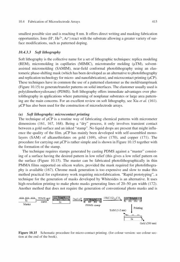
(a) Soft lithography: microcontact printingThe technique of �CP is a routine way of fabricating chemical patterns with micrometerdimensions (161, 167, 168). Being a “dry” process, it only involves transient contactbetween a gold surface and an inked “stamp”. No liquid drops are present that might influ-ence the quality of the film. �CP has mainly been developed with self-assembled mono-layers (SAM) of alkanethiolates on gold (169), silver (170), and copper (171). Theprocedure for carrying out �CP is rather simple and is shown in Figure 10.15 together withthe formation of the stamp.
The technique requires stamps generated by casting PDMS against a “master” consist-ing of a surface having the desired pattern in low relief (this gives a low relief pattern onthe surface (Figure 10.15). The master can be fabricated photolithographically in thinPMMA films supported on silicon wafers, provided the mask required for photolithogra-phy is available (167). Chrome mask generation is too expensive and slow to make thismethod practical for exploratory work requiring microfabrication. “Rapid prototyping”, atechnique for the generation of masks developed by Whitesides is an alternative. It useshigh-resolution printing to make photo masks generating lines of 20–50 �m width (172).Another method that does not require the generation of conventional photo masks and is
10.4 Fabrication of Microelectrode Arrays 415
Figure 10.15 Schematic procedure for micro-contact printing. (for colour version: see colour sec-tion at the end of the book).
Ch010.qxd 10/20/2006 3:37 PM Page 415
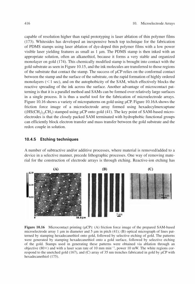
capable of resolution higher than rapid prototyping is laser ablation of thin polymer films(173). Whitesides has developed an inexpensive bench top technique for the fabrication of PDMS stamps using laser ablation of dye-doped thin polymer films with a low powervisible laser yielding features as small as 1 �m. The PDMS stamp is then inked with anappropriate solution, often an alkanethiol, because it forms a very stable and organizedmonolayer on gold (174). This chemically modified stamp is brought into contact with thegold substrate as seen in Figure 10.15, and the ink molecules are transferred to those regionsof the substrate that contact the stamp. The success of �CP relies on the conformal contactbetween the stamp and the surface of the substrate, on the rapid formation of highly orderedmonolayers (�1 sec), and on the autophobicity of the SAM, which effectively blocks thereactive spreading of the ink across the surface. Another advantage of microcontact pat-terning is that it is a parallel method and SAMs can be formed over relatively large surfacesin a single process. It is thus a useful tool for the fabrication of microelectrode arrays.Figure 10.16 shows a variety of micropatterns on gold using �CP. Figure 10.16A shows thefriction force image of a microelectrode array formed using hexadecylmercaptane((HS(CH2)15CH3) stamped using �CP onto gold (41). The key point of SAM-based micro-electrodes is that the closely packed SAM terminated with hydrophobic functional groupscan efficiently block electron transfer and mass transfer between the gold substrate and theredox couple in solution.
10.4.5 Etching techniques
A number of subtractive and/or additive processes, where material is removed/added to adevice in a selective manner, precede lithographic processes. One way of removing mate-rial for the construction of electrode arrays is through etching. Reactive-ion etching has
416 10. Microelectrode Arrays
Figure 10.16 Microcontact printing (�CP): (A) friction force image of the prepared SAM-basedmicroelectrode array 1 �m in diameter and 5 �m in pitch (41); (B) optical micrograph of lines pat-terned by stamping hexadecanethiol onto gold, followed by selective etching of gold. The patternswere generated by stamping hexadecanethiol onto a gold surface, followed by selective etching of the gold. Stamps used in generating these patterns were obtained via ablation through an objective (80�) and with a laser scan rate of 10 mm min�1, power 10 mW. The white regions cor-respond to the unetched gold (167), and (C) array of 35 nm trenches fabricated in gold by �CP withhexadecanethiol (175).
Ch010.qxd 10/20/2006 3:37 PM Page 416
been discussed. However, subtractive etching techniques range from wet etching, electro-chemical etching, photo-electrochemical etching to focused ion-beam milling, plasmaetching, laser machining, ultrasonic drilling, and mechanical methods (160).
Chemical etching has been widely used for the fabrication of three-dimensional micro-electrode arrays. These kinds of electrode array configurations have been widely used toexplore and assess intracortical brain activity (176). It is widely accepted that the cerebralcortex provides the easiest access to motor intent and sensory perception and is thus anattractive region for interfacing potential future devices for restoring neurological func-tions lost due to degenerative muscular diseases, strokes, or spinal cord injury (177). Muchis still unknown about the generation of different motor behaviors, but it has been recog-nized that for clinical applications of such “brain-machine” interfaces, the activities ofhundreds of thousands of neurons must be simultaneously sampled. A three-dimensionalelectrode array allows capturing neural signals from a collection of recording sites with a pre-selected spatial distribution. Two well-known approaches include the developmentof microelectrode arrays at the University of Utah (178, 179) and at the University ofMichigan (180). Fofonoff reported the fabrication of a three-dimensional array by electri-cal discharge machining followed by chemical etching (181). To reduce the dimensions ofthe micromachined array, it was placed into a hot HCl bath heated close to its boiling point(Figure 10.17A). Electroplating with gold followed by platinum and final electrical insu-lation into parylene formed an array of platinum-coated electrodes (Figure 10.17B).
A rather different approach for the fabrication of three-dimensional electrode arraysis based on the use of optical imaging fiber arrays. An imaging fiber array has thousandsof individual optical fibers (diameter of 3–4 �m) melted and drawn together in a coher-ent way. This imaging fiber can be used as a platform for the construction of a three-dimensional electrode array through chemical etching of the optical fibers. In the case ofa silica fiber, the optical fiber is chemically etched in one-step procedure by dipping thefiber array into a solution of hydrofluoric acid (160) and ammonium fluoride (NH4F)buffer (34, 182). The fiber’s etch rate is dependent on the dopant concentration in thefiber and the concentration of the acid solution. In the case of the fibers used by Walt et al.,etching occurs at different rates between the pure SiO2 of the fiber cladding and the GeO2
doped SiO2 of the core (Figure 10.17B1). The chemical reaction of SiO2 and GeO2 withHF acid can be summarized by reactions (10.8)–(10.10). The fluorosilicic acid (H2SiF6)
10.4 Fabrication of Microelectrode Arrays 417
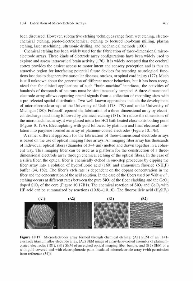
Figure 10.17 Microelectrodes array formed through chemical etching. (A1) SEM of an 1141-electrode titanium alloy electrode array, (A2) SEM image of a parylene-coated assembly of platinum-coated electrodes (181), (B1) SEM of an etched optical imaging fiber bundle, and (B2) SEM of awith gold covered and with electrophoretic paint insulated microelectrode array (with permissionfrom reference (34)).
Ch010.qxd 10/20/2006 3:37 PM Page 417
and the hexafluorogermanic acid (H2GeF6) is produced either directly (reactions (10.8a)and (10.8b)) or as outlined by reactions (10.9)–(10.11).
(10.8a)
(10.8b)
(10.9a)
(10.9b)
(10.10a)
(10.10b)
If an ammonium fluoride buffered etching solution is used, there is a further possible dis-solution step involved, which arises from the involvement of ammonic ionized from thesolution (reactions (10.11a) and (10.11b)).
(10.11a)
(10.11b)
It is the difference in the solubility of the resultant (NH4)2SiF6 and (NH4)2GeF6, whichleads to the difference in etching rates between the core and cladding. The tip cone angleis thus primarily a function of the etching solution and the GeO2 doping level of the fibercore, while the temperature, the type, and concentration of the acid used, and the etchingtime are crucial for the optical and geometrical characteristics (such as cone angle andaperture diameter) of the tips formed. An ordered array of individual microelectrodes (6 �m center-to-center spacing) was fabricated by coating such a chemically etched imag-ing fiber bundle with gold and insulating the base of the fiber array with an electrophoreticpaint. Electrophoretic paints have been shown to be useful for the fabrication of micro-electrodes (183, 184). The electrophoretic paint consists mainly of two types of resins:polyacrylates and polyurethanes, where the cross-linking reaction is between the iso-cyanate group on the urethane resins and the hydroxyl groups in the polyacrylates. Theprinciple mechanism of deposition is by depletion of hydrogen ions at the cathode viaapplication of a positive DC voltage between the cathode (fiber bundle) and the anode (Cuwire). The resulting increase in pH destabilizes the cationic resin emulsion and the resinloses the colloidal condition and deposits onto the cathodic surface. Curing the fiber sub-sequently at 200 �C results in the shrinking of the deposited film and insures that the tipapex is not covered (Figure 10.17B2).
10.5 ELECTROCHEMICAL CHARACTERISATION OF
MICROELECTRODE ARRAYS
Microelectrode arrays are generally characterized using a combination of voltammetry,SEM, and atomic force microscopy (185, 186). In addition to these techniques, othermethods are reported which have been shown to be important in characterizing in situ the
H GeF NH NH GeF2 6 3 4 2 62+ → ( )
H SiF NH NH SiF2 6 3 4 2 62+ → ( )
3 2 24 2 2 6 2GeF H O H GeF GeO aq+ → + ( )
GeO HF GeF H O2 4 24 2+ → +
3 2 24 2 2 6 2SiF H O H SiF SiO aq+ → + ( )
SiO HF SiF H O2 4 24 2+ → +
GeO HF H GeF H O2 2 6 26 2+ → +
SiO HF H SiF H O2 2 6 26 2+ → +
418 10. Microelectrode Arrays
Ch010.qxd 10/20/2006 3:37 PM Page 418
electrochemical reactivities of ensembles of microelectrodes operating at the same poten-tial or addressed individually.
10.5.1 Chronoamperometry and cyclic voltammetry
For a microelectrode array, chronoamperometric responses are complex and depend on thetime frame of the experiment and the limiting behaviors described in section 10.3.1 (26).In the case of a regular ensemble of electrodes, the general trend of the chronoampero-metric response is well known. At short times, the array behaves as individual electrodesand the response to a potential step shows planar diffusion (Cottrellian behavior withdependence of the current as 1/√(�) since no interference from overlapping diffusionoccurs. At longer times, this behavior changes to a mixed regime where hemispherical dif-fusion prevails and this regime is finally converted again to one of planar diffusion. In thislast case, the diffusion layers fully overlap and the entire array behaves as a macroelec-trode whose area is equal to the total geometric surface area (see Section 10.3.1).
An analytical expression for the current was provided by Shoup and Szabo (106) for aninfinite number of microdisk interfaces operating at the same potential in a hexagonalarray:
(10.12)
where � is the dimensionless time with � = 4Dt/r2, � the array coverage with � - (2r/d)2, rthe radius of the microdisks, d the center-to-center distance between microdisks, and B aconstant equal to 0.7823. At short times, the predicted currents follow the Cottrell equa-tion given for linear diffusion to the area of a single microdisk (i.e., �r2), while at longertimes, they converge to the Cottrell equation corresponding to linear diffusion to the totalgeometric area (i.e., �d2/4). The characteristic time corresponding to a nonlinear to a lin-ear transition from when diffusion layers overlap depends on both the size of the individ-ual microelectrodes and their packing in the array as well as on the diffusion coefficient ofredox species. This time tc can be evaluated by (106)
(10.13)
However, equation 10.13 is not always experimentally appropriate (187) and gives only acrude estimation of the transition time tc when individual diffusion layers begin to overlapaccording to the packing density of the array. Similar results have been also derived froma simple analytical approach to hexagonal, square, and random arrays (21). It must beemphasized that all these approaches remain valid over a specific range of parameters
td r
Dc =−( / )2
6
2
fi
nFrDC
B( , ) exp
( )
exp
*� �
�
�
� � � �
�= + + −
4 2 41
4
3 22
=
− −
− −
�� ��
�� �
�
��
��
2 11
43 2
13
2 1
23−
+ −
−
+−
B ( )
( ))
−1
10.5 Electrochemical Characterisation of Microelectrode Arrays 419
Ch010.qxd 10/20/2006 3:37 PM Page 419
resulting from particular assumptions or approximations (see Section 10.3.1). For exam-ple, numerical simulations of chronoamperometric responses of infinite arrays (110)showed that equation 10.12 was valid only for values of � exceeding 0.9. The electro-chemical properties depend strongly on the way the microelectrodes are packed as arraysof recessed microelectrodes behave differently from arrays of inlaid electrodes in the shortand medium time domains (110).
The interpretation of the response of an assembly of microelectrodes to a cyclic voltam-metric waveform is more complicated than in the case of chronoamperometry. Whenapplied to microelectrode arrays, it is mainly used in the steady-state limit. From an elec-troanalytical point of view, the major issue is to choose an appropriate scan rate � to ensuresteady-state diffusion at the array interface. If the scan rate is not properly chosen, a peak-shaped voltammogram is observed whose characteristics can be derived only from simu-lations (188). Figure 10.18 shows simulated cyclic voltammograms obtained at an infinitenumber of microdisks (r = 10 �m) in a hexagonal array with d/r ranging from 3 to 100and d ranging from 20 to 1000 �m.
Two characteristic polarization curves can be observed. In the case of high d/r ratios,a sigmoidal shape is related to the individual mipcrodisk electrode behavior (hemi-spherical diffusion). As in the case of low d/r ratios, a peak-shaped voltammogram isobtained corresponding to linear diffusion. For intermediate d/r ratios, a mixed diffusion
420 10. Microelectrode Arrays
Figure 10.18 Simulated cyclic voltammograms obtained at an infinite number of microdisks in a hexagonal array having various interelectrode (center-to-center) distance, d. d/r = 3–100, � = 10 mV sec�1, r = 10 �m, D = 10�7 cm2 sec�1 (with permission from reference (188)).
Ch010.qxd 10/20/2006 3:37 PM Page 420
regime takes place where the current slowly increases with d/r and the peak separationwidens. Moreover, the peak-to-peak separation becomes larger in the same way as whenthe apparent electron transfer process is lowered, even if a Nernstian system is assumedduring simulation. The characteristic scan rate � from which a steady-state voltammo-gram is observed can be easily derived from equation 10.12 as the equivalency involtammetry between time and scan rate is straightforward (i.e., tc = RT/F�). This behav-ior has been predicted by Amatore et al. (14) for charge transfer at partially blockedelectrodes (see Section 10.3.1). The shapes and characteristics of the voltammogramscan be deduced from a zone diagram (Figure 10.19), which defines four main domainswhere different characteristic behaviors are encountered. Vertical frontiers delimit thelinear and spherical diffusion fields. From the upper side to the lower side, a distinctionis made between voltammograms exhibiting either a fast electron transfer or an appar-ent quasi-irreversible electron transfer. This zone diagram shows clearly the stronginfluence of the fractional coverage or packing density of the array on the apparent stan-dard rate constant of the electrochemical reaction. It can be easily derived for a hexag-onal array of microdisk electrodes with the assumption of disk inactive sites rather thanhexagonal ones (188).
10.5 Electrochemical Characterisation of Microelectrode Arrays 421
Figure 10.19 Zone diagram representing the main characteristics of cyclic voltammograms as a func-tion of two dimensionless parameters, K�1/2 and (1 � �) with
and . � represents the fractional coverage ofthe insulating sites and is defined as with Sins and Sact the insulating and electro-active surface areas, respectively. k is the standard rate constant for the electron transfer at the active site.tc = RT/F� with � the scan rate. Adapted from reference (14).
� = +S S Sins ins act/( )Λ − = −( ) ( / ) ( )/1 11 2� �k t Dct� 1 2 1 21 0 27 1 / /ln[ . ( ) ]]−+ −
cc1 2/
K D d� � � � �1 2 2 1 11 8 1/ [( ) ][( ) ( )= − −− −/ / /
Ch010.qxd 10/20/2006 3:37 PM Page 421
10.5.2 Scanning electrochemical microscopy
Scanning electrochemical microscopy (SECM) is commonly used to characterize differentsubstrates and microelectrodes as well as to image their interfaces (189). For a moredetailed discussion about SECM see Chapter 12. In comparison to conventional micro-scopies, this method gives valuable information regarding the conductivity, connectivity,and reactivity of microelectrode arrays (190). It can be used not only to map microelec-trode arrays or track patterns but also to determine at the same time the integrity of theinsulator coatings. Different SECM modes can be used depending on whether the micro-electrodes in the array and the tips used for imaging the surface are reciprocally biased orunbiased. The feedback and the substrate generation/tip collection (SG/TC) modes ofSECM were found to address each of these issues (190). The features of these two SECMmodes have found to be particularly useful when random microelectrode arrays are beingfabricated and characterized.
10.5.3 Optical microscopy
Information about the geometry, homogeneity, and morphology of array surfaces may beobtained from scanning methods, like AFM, STM, SECM, or SEM. However, these meth-ods are not capable of giving direct evidence of the electrochemical activities of micro-electrodes in arrays. Except for SECM, one way to overcome this difficulty is to detectoptically the ECL initiated on each microelectrode. Indeed, by placing the microelectrodearray under an optical microscope fitted with a high sensitivity CCD camera, ECL imagescan be acquired from the focal plane, which are directly correlated to the electrochemicalactivities of each microelectrode of the array (34). Furthermore, according to the mecha-nism of the ECL reaction involved, the size of the individual diffusion layers can be eval-uated from the size of the ECL spots, which in turn, gives an estimation of the electrodedimension. The resolution achieved by this method allows the imaging of sub-micrometerelectrodes.
Another way to characterize the electrochemical activity of microelectrode arrays is tomap the electroactive species generated at each electrode by confocal Raman spec-troscopy. Indeed, the use of confocal signal detection enables Raman spectroscopic meas-urements of very small sample volumes (even down to a few �m3). Applied to amicroelectrode array, it provides a statistical picture of the distribution of active sites onthe array (60). As in the case of SECM, these two optical methods are particularly usefulto verify if individual diffusion layers do not overlap and if the microelectrodes in the arrayare diffusely independent, particularly for random microelectrode arrays.
10.6 CONCLUSION AND PROSPECTS
Microelectrode arrays have been widely discussed in the literature from theoretical andpractical viewpoints and these have led to a better understanding of typical characteristicsencountered during their operation. Such devices offer advantages in a number of areas of
422 10. Microelectrode Arrays
Ch010.qxd 10/20/2006 3:37 PM Page 422
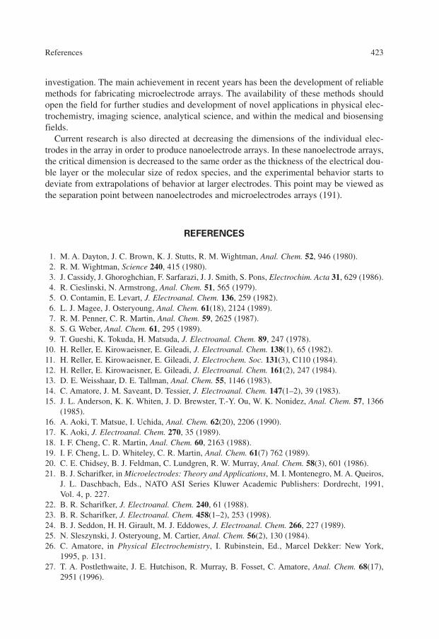
investigation. The main achievement in recent years has been the development of reliablemethods for fabricating microelectrode arrays. The availability of these methods shouldopen the field for further studies and development of novel applications in physical elec-trochemistry, imaging science, analytical science, and within the medical and biosensingfields.
Current research is also directed at decreasing the dimensions of the individual elec-trodes in the array in order to produce nanoelectrode arrays. In these nanoelectrode arrays,the critical dimension is decreased to the same order as the thickness of the electrical dou-ble layer or the molecular size of redox species, and the experimental behavior starts todeviate from extrapolations of behavior at larger electrodes. This point may be viewed asthe separation point between nanoelectrodes and microelectrodes arrays (191).
REFERENCES
1. M. A. Dayton, J. C. Brown, K. J. Stutts, R. M. Wightman, Anal. Chem. 52, 946 (1980).2. R. M. Wightman, Science 240, 415 (1980).3. J. Cassidy, J. Ghoroghchian, F. Sarfarazi, J. J. Smith, S. Pons, Electrochim. Acta 31, 629 (1986).4. R. Cieslinski, N. Armstrong, Anal. Chem. 51, 565 (1979).5. O. Contamin, E. Levart, J. Electroanal. Chem. 136, 259 (1982).6. L. J. Magee, J. Osteryoung, Anal. Chem. 61(18), 2124 (1989).7. R. M. Penner, C. R. Martin, Anal. Chem. 59, 2625 (1987).8. S. G. Weber, Anal. Chem. 61, 295 (1989).9. T. Gueshi, K. Tokuda, H. Matsuda, J. Electroanal. Chem. 89, 247 (1978).
10. H. Reller, E. Kirowaeisner, E. Gileadi, J. Electroanal. Chem. 138(1), 65 (1982).11. H. Reller, E. Kirowaeisner, E. Gileadi, J. Electrochem. Soc. 131(3), C110 (1984).12. H. Reller, E. Kirowaeisner, E. Gileadi, J. Electroanal. Chem. 161(2), 247 (1984).13. D. E. Weisshaar, D. E. Tallman, Anal. Chem. 55, 1146 (1983).14. C. Amatore, J. M. Saveant, D. Tessier, J. Electroanal. Chem. 147(1–2), 39 (1983).15. J. L. Anderson, K. K. Whiten, J. D. Brewster, T.-Y. Ou, W. K. Nonidez, Anal. Chem. 57, 1366
(1985).16. A. Aoki, T. Matsue, I. Uchida, Anal. Chem. 62(20), 2206 (1990).17. K. Aoki, J. Electroanal. Chem. 270, 35 (1989).18. I. F. Cheng, C. R. Martin, Anal. Chem. 60, 2163 (1988).19. I. F. Cheng, L. D. Whiteley, C. R. Martin, Anal. Chem. 61(7) 762 (1989).20. C. E. Chidsey, B. J. Feldman, C. Lundgren, R. W. Murray, Anal. Chem. 58(3), 601 (1986).21. B. J. Scharifker, in Microelectrodes: Theory and Applications, M. I. Montenegro, M. A. Queiros,
J. L. Daschbach, Eds., NATO ASI Series Kluwer Academic Publishers: Dordrecht, 1991, Vol. 4, p. 227.
22. B. R. Scharifker, J. Electroanal. Chem. 240, 61 (1988).23. B. R. Scharifker, J. Electroanal. Chem. 458(1–2), 253 (1998).24. B. J. Seddon, H. H. Girault, M. J. Eddowes, J. Electroanal. Chem. 266, 227 (1989).25. N. Sleszynski, J. Osteryoung, M. Cartier, Anal. Chem. 56(2), 130 (1984).26. C. Amatore, in Physical Electrochemistry, I. Rubinstein, Ed., Marcel Dekker: New York,
1995, p. 131.27. T. A. Postlethwaite, J. E. Hutchison, R. Murray, B. Fosset, C. Amatore, Anal. Chem. 68(17),
2951 (1996).
References 423
Ch010.qxd 10/20/2006 3:37 PM Page 423

28. G. Kindlman, R. A. Normann, A. Badi, J. Bigler, C. Keller, R. Coffey, G. M. Jones, C. R. Johnson,BISTI 2003 Symposium, Digital Biology: The Ermging Paradigm, www.bisti.nih.gov/2003meeting (2003).
29. W. L. Caudill, J. O. Howell, R. M. Wightman, Anal. Chem. 54, 2532 (1982).30. P. Bindra, A. P. Brown, M. Fleischmann, D. Pletcher, J. Electroanal. Chem. 58, 31 (1975).31. P. Bindra, J. Ulstrup, J. Electroanal. Chem. 140, 131 (1982).32. E. Sabatini, I. Rubinstein, J. Phys. Chem. 91, 6663 (1987).33. E. Sabatini, I. Rubinstein, R. Maoz, J. Sagiv, J. Electroanal. Chem. 219, 365 (1987).34. S. Szunerits, J. M. Tam, L. Thouin, C. Amatore, D. R. Walt, Anal. Chem. 75(17), 4382 (2003).35. S. Szunerits, D. R. Walt, Anal. Chem. 74(7), 1718 (2002).36. S. Szunerits, D. R. Walt, Chemphyschem 4(2), 186 (2003).37. A. Chovin, P. Garrigue, P. Vinatier, N. Sojic, Anal. Chem. 76(2), 357 (2004).38. M. DeAbreu, W. C. Purdy, Anal. Chem. 59(1), 204 (1987).39. H. Ecken, S. Ingebrandt, M. Krause, D. Richter, M. Hara, A. Offenhauser, Electrochim. Acta 48,
3355 (2003).40. G. C. Fiaccabrino, M. Koudelkahep, S. Jeanneret, A. Vandenberg, N. F. Derooij, Sens. Actuat. B
Chem. 19(1–3), 675 (1994).41. H. X. He, Q. G. Li, Z. Y. Zhou, H. Zhang, S. F. Y. Li, Z. F. Liu, Langmuir 16(25), 9683 (2000).42. F. Heer, W. Franks, A. Blau, S. Taschini, C. Ziegler, A. Hierlemann, H. Baltes, Biosens.
Bioelectron. 20, 358 (2004).43. Y. Iwasaki, O. Niwa, M. Morita, H. Tabei, P. T. Kissinger, Anal. Chem. 68(21), 3797 (1996).44. S. P. Kounaves, W. Deng, P. R. Hallock, G. T. A. Kovacs, C. W. Storment, Anal. Chem. 66(3),
418 (1994).45. H. J. Lee, C. Beriet, H. H. Girault, J. Electroanal. Chem. 453, 211 (1998).46. J. Pei, M. L. Tercier-Waeber, J. Buffle, G. C. Fiaccabrino, M. Koudelka-Hep, Anal. Chem. 73,
2273 (2001).47. B. J. Seddon, C. F. Wang, W. F. Peng, X. J. Zhang, J. Chem. Soc.-Faraday Trans. 90(4), 605 (1994).48. C. Amatore, C. Sella, L. Thouin, J. Phys. Chem. B 106(44), 11565 (2002).49. I. B. Svir, A. I. Oleinick, R. G. Compton, J. Electroanal. Chem. 560(2), 117 (2003).50. C. Amatore, M. Belotti, Y. Chen, E. Roy, C. Sella, L. Thouin, J. Electroanal. Chem. 573, 333 (2004).51. C. Amatore, L. Thouin, J.-S. Warkocz, Chem. Eur. J. 5(2), 456 (1999).52. I. A. Arkoub, C. Amatore, C. Sella, L. Thouin, J. S. Warkocz, J. Phys. Chem. B 105(37), 8694
(2001).53. B. Fosset, C. A. Amatore, J. E. Bartelt, A. C. Michael, R. M. Wightman, Anal. Chem. 63(4), 306
(1991).54. T. V. Shea, A. J. Bard, Anal. Chem. 59(17), 2101 (1987).55. C. Amatore, A. R. Brown, J. Am. Chem. Soc. 118, 1482 (1996).56. J. E. Bartelt, M. R. Deakin, C. A. Amatore, R. M. Wightman, Anal. Chem. 60, 2167 (1988).57. H. A. O. Hill, N. A. Klein, I. S. M. Psalti, N. J. Walton, Anal. Chem. 61, 2200 (1989).58. R. G. Compton, B. A. Coles, J. J. Gooding, A. C. Fisher, T. I. Cox, J. Phys. Chem. 98, 2446
(1994).59. J. H. Thomas, S. K. Kim, P. J. Hesketh, H. B. Halsall, W. R. Heineman, Anal. Biochem. 328(2),
113 (2004).60. L. J. Yang, Y. B. Li, G. F. Erf, Anal. Chem. 76(4), 1107 (2004).61. J. Senior, A. Shah, C. Monteux, V. De Biasi, J. Pharm. Biomed. Anal. 24(5–6), 843 (2001).62. R. Kurita, H. Tabei, Z. M. Liu, T. Horiuchi, O. Niwa, Sens. Actuat. B Chem. 71(1–2), 82 (2000).63. R. M. Blanchard, A. R. Noble-Luginbuhl, R. G. Nuzzo, Anal. Chem. 72(7), 1365 (2000).64. O. Niwa, R. Kurita, Z. M. Liu, T. Horiuchi, K. Torimitsue, Anal. Chem. 72(5), 949 (2000).65. M. P. Nagale, I. Fritsch, Anal. Chem. 70(14), 2902 (1998).
424 10. Microelectrode Arrays
Ch010.qxd 10/20/2006 3:37 PM Page 424

66. M. Morita, O. Niwa, T. Horiuchi, Electrochim. Acta 42(20–22), 3177 (1997).67. M. Morita, O. Niwa, Nat. Rev. 8(2), 77 (1996).68. S. Hoshino, O. Niwa, H. Tabei, M. Takahashi, M. Morita, Denki Kagaku 64(3), 195 (1996).69. O. Niwa, Electroanalysis 7(7), 606 (1995).70. M. Paeschke, U. Wollenberger, C. Kohler, T. Lisec, U. Schnakenberg, R. Hintsche, Anal. Chim.
Acta 305(1–3), 126 (1995).71. O. Niwa, T. Horiuchi, H. Tabei, J. Electroanal. Chem. 367(1–2), 265 (1994).72. O. Niwa, M. Morita, H. Tabei, Electroanalysis 6(3), 237 (1994).73. O. Niwa, H. Tabei, Anal. Chem. 66(2), 285 (1994).74. A. J. Bard, J. A. Crayston, G. P. Kittlesen, T. V. Shea, M. S. Wrighton, Anal. Chem. 58(11),
2321 (1986).75. J. A. Alden, M. A. Feldman, E. Hill, F. Prieto, M. Oyama, B. A. Coles, R. G. Compton,
P. J. Dobson, P. A. Leigh, Anal. Chem. 70(9), 1707 (1998).76. K. Aoki, M. Morita, O. Niwa, H. Tabei, J. Electroanal. Chem. 256, 269 (1988).77. K. Aoki, M. Tanaka, J. Electroanal. Chem. 266, 11 (1989).78. B. J. Feldman, R. W. Murray, Anal. Chem. 58(13), 2844 (1986).79. B. J. Feldman, R. W. Murray, Inorg. Chem. 26, 1702 (1987).80. O. Niwa, M. Morita, H. Tabei, Anal. Chem. 62(5), 447 (1990).81. O. Niwa, Y. Xu, H. B. Halsall, W. R. Heineman, Anal. Chem. 65, 1559 (1993).82. O. Niwa, M. Morita, Anal. Chem. 68(2), 355 (1996).83. L. E. Fosdick, J. L. Anderson, Anal. Chem. 58(12), 2481 (1986).84. R. Merletti, D. Farina, M. Gazzoni, J. Electromyogr. Kinesiol. 13, 37 (2003).85. T. Masuda, H. Miyano, T. Sadoyama, Electroencephalogr. Clin. Neurophysiol. 56, 597
(1983).86. S. Szunerits, P. Garrigue, J.-L. Bruneel, L. Servant, N. Sojic, Electroanalysis 15, 548 (2003).87. T. E. McKnight, A. V. Melechko, D. W. Austin, T. Sims, M. A. Guillorn, M. L. Simpson,
J. Phys. Chem. B 108(22), 7115 (2004).88. S. Fletcher, in Microelectrodes: Theory and Applications, M. I. Montenegro, M. A. Querios,
J. L. Daschbach, Eds., Kluwer: Dordrecht, 1991, p. 342.89. S. Fletcher, M. D. Horne, Electrochem. Commun. 1(10), 502 (1999).90. P. Connolly, G. R. Moores, W. Monagham, J. Shen, S. Britland, P. Clark, Sens. Actuat. B6, 113
(1992).91. D. W. Deer, C. W. Toblas, J. Electrochem. Soc. 134, 369 (1987).92. M. G. Sullivan, H. Utomo, P. J. Fagan, M. D. Ward, Anal. Chem. 71, 4369 (1999).93. T. Livache, H. Bazin, P. Caillat, A. Roget, Biosens. Bioelectr. 13, 629 (1998).94. C. Berloment, M.-L. Tercier, J. Buffle, G. C. Fiaccabrino, M. Koudelka-Hep, Anal. Chim. Acta
329, 203 (1996).95. Q. Bai, K. D. Wise, Trans. Biomed. Eng. 48(8), 911 (2001).96. J. J. Pancrazio, J. P. P. Bey, D. S. Cuttino, J. K. Kusel, D. A. Borkholder, K. M. Shaffer,
G. T. A. Kovacs, D. A. Stenger, Sens. Actuat. B53, 179 (1998).97. N. H. E. Weste, K. Eshraghian, Principles of Cmos Vlsi Design, Addison Wesley: Reading,
MA, 1994.98. L. Berdondini, P. D. van der Wal, N. F. de Rooij, A. Koudelka-Hep, Sens. Actuat. B Chem.
99(2–3), 505 (2004).99. L. E. Fosdick, J. L. Anderson, T. A. Baginski, R. C. Jaeger, Anal. Chem. 58, 2750 (1986).
100. K. Aoki, J. Osteryoung, J. Electroanal. Chem. 125, 315 (1981).101. T. Gueshi, K. Tokuda, J. Matsuda, J. Electroanal. Chem. 101, 29 (1979).102. W. Thormann, P. v. d. Bosch, A. M. Bond, Anal. Chem. 57(14), 2764 (1985).103. K. Tokuda, T. Gueshi, H. Matsuda, J. Electroanal. Chem. 102(1), 41 (1979).
References 425
Ch010.qxd 10/20/2006 3:37 PM Page 425

104. E. Levart, D. Schauhmann, E. Contamin, M. Etman, J. Electroanal. Chem. 70, 117 (1976).105. J. Lindemann, R. Landsberg, J. Electroanal. Chem. 30, 79 (1971).106. D. Shoup, A. Szabo, J. Electroanal. Chem. 160(1–2), 19 (1984).107. B. A. Brookes, T. J. Davies, A. C. Fisher, R. G. Evans, S. J. Wilkins, K. Yunnus, J. D. Wadhawan,
R. G. Compton, J. Phys. Chem. B 107, 1616 (2003).108. T. J. Davies, B. A. Brookes, A. C. Fisher, K. Yunnus, S. J. Wilkins, P. R. Greene, J. D. Wadhawan,
R. G. Compton, J. Phys. Chem. B 107, 6431 (2003).109. A. Szabo, R. Zwanzig, J. Electroanal. Chem. 314, 307 (1991).110. C. Beriet, R. Ferrigno, H. H. Girault, J. Electroanal. Chem. 486(1), 56 (2000).111. W. E. Morf, Anal. Chim. Acta 330(2–3), 139 (1996).112. S. D. Kolev, J. H. M. Simons, W. E. Vanderlinden, Anal. Chim. Acta 273(1–2), 71 (1993).113. B. Fosset, C. Amatore, J. Bartelt, R. M. M. Wightman, Anal. Chem. 63, 1403 (1991).114. A. I. Oleinick, I. B. Svir, C. Amatore, J. Electroanal. Chem. 553, 49 (2003).115. T. Horiuchi, O. Niwa, M. Morita, J. Electroanal. Chem. 142(9), L146 (1995).116. V. P. Menon, C. R. Martin, Anal. Chem. 67, 1920 (1995).117. M. P. Nagale, I. Fritsch, Anal. Chem. 70, 2908 (1998).118. D. M. Odell, W. J. Bowyer, Anal. Chem. 62(15), 1619 (1990).119. M. Ohtani, T. Sunagawa, S. Kuwabata, H. Yoneyyama, J. Electroanal. Chem. 396, 97 (1995).120. J. L. Anderson, L. A. Coury, J. Leddy, Anal. Chem. 70(12), 516R (1998).121. O. T. Guenat, J.-F. Dufour, P. D. van der Wal, W. E. Morf, N. F. de Rooij, M. Koudelka-Hep,
Sens. Actuat. B 105, 65 (2005).122. J. J. Hickman, C. Zou, D. Ofer, P. D. Harvey, M. S. Wrighton, J. Am. Chem. Soc. 111, 7271
(1989).123. S. K. Kim, P. J. Hesketh, C. Li, J. H. Thomas, H. B. Halsall, W. R. Heinemann, Biosens.
Bioelectr. 20, 887 (2004).124. G. P. Kittlesen, H. S. White, M. S. Wrighton, J. Am. Chem. Soc. 106, 7389 (1984).125. C. D. Merritt, B. L. Justus, Chem. Mater. 15(13), 2520 (2003).126. E. W. Paul, A. J. Ricco, M. S. Wrighton, J. Phys. Chem. 89, 1441 (1985).127. B. J. Seddon, M. J. Eddowes, A. Firth, A. E. Owen, H. H. J. Girault, Electrochim. Acta 36(5–6),
763 (1991).128. G. Sreenivas, S. S. Ang, I. Fritsch, W. D. Brown, G. A. Gerhardt, D. J. Woodward, Anal. Chem.
68(11), 1858 (1996).129. K. D. Sternitzke, R. L. McCreery, Anal. Chem. 62(13), 1339 (1990).130. H. Suzuki, Electroanalysis 12(9), 703 (2000).131. K. Tsunozaki, Y. Einaga, T. N. Rao, A. Fujishima, Chem. Lett. 5, 502 (2002).132. H. S. White, G. P. Kittlesen, M. S. Wrighton, J. Am. Chem. Soc. 106, 5375 (1984).133. H. P. Wu, Anal. Chem. 65(11), 1643 (1993).134. H. Xiong, J. D. Guo, K. Kurihara, S. Amemiya, Electrochem. Commun. 6(6), 615 (2004).135. R. M. Wightman, D. O. Wipf, in Electroanalytical Chemistry, A. J. Bard, Ed., Marcel Dekker:
New York, 1989, Vol. 15, p. 267.136. A. C. Barton, S. D. Collyer, F. Davis, D. D. Gornall, K. A. Lawa, E. C. D. Lawrence, D. W. Mills,
S. Myler, J. A. Pritchard, M. Thompsonc, S. P. J. Higson, Biosens. Bioelectr. (2004).137. J. Schwarz, H. Kaden, U. Enseleit, Electrochem. Commun. 2, 606 (2000).138. P. J. Welford, J. Freeman, S. J. Wilkins, J. D. Wadhawan, C. E. W. Hahn, R. G. Compton, Anal.
Chem. 73, 6088 (2001).139. B. K. Davis, S. G. Weber, A. P. Sylwesert, Anal. Chem. 62, 1000 (1990).140. C. R. Martin, Science 266, 1961 (1994).141. G. L. Hornay, C. J. Patrissi, C. R. Martin, J. Phys. Chem. B 101, 1548 (1997).142. W. E. Williams, N. Giordano, Rev. Sci. Instrum. 55, 410 (1984).
426 10. Microelectrode Arrays
Ch010.qxd 10/20/2006 3:37 PM Page 426

143. R. L. Fleischer, P. B. Price, R. M. Walker, Nuclear Tracks in Solids, University of CaliforniaPress: Berkeley, CA, 1975.
144. P. P. Ngugen, D. H. Pearson, R. J. Tonucci, K. Babcock, J. Electrochem. Soc. 145, 247 (1998).145. G. E. Possin, Rev. Sci. Instrum. 41, 772 (1970).146. K. Hiruma, M. Yazawa, T. Katsuyama, K. Ogawa, K. Haraguchi, M. Koguchi, H. Kakibayashi,
J. Appl. Phys. 77, 447 (1995).147. C. A. Huber, T. E. Huber, M. Sadoqi, J. A. Lubin, S. Manalis, C. B. Prater, Science 263, 800
(1994).148. C. R. Martin, Adv. Mater. 3, 457 (1991).149. C. R. Martin, Acc. Chem. Res. 28, 61 (1995).150. Y.-L. Tai, H. Teng, Chem. Mater. 16, 338 (2004).151. J. C. Hulteen, K. B. Jirage, C. R. Martin, J. Am. Chem. Soc. 120, 6603 (1998).152. S. Valizadeh, J. M. George, P. Leisner, L. Hultman, Electrochim. Acta 47(6), 865 (2001).153. B. B. Lakshmi, C. J. Patrissi, C. R. Martin, Chem. Mater. 9, 2544 (1997).154. S. A. Miller, V. Y. Young, C. R. Martin, J. Am. Chem. Soc. 123, 12335 (2001).155. P. C. Hidberg, P. F. Nealey, W. Helbig, G. M. Whitesides, Langmuir 12, 5209 (1996).156. Z. Hou, S. Dante, N. Abbott, P. Stroeve, Langmuir 15, 3011 (1999).157. S. Metzer, R. Resch, B. E. Koel, M. E. Thompson, A. Madhukar, A. A. G. Requicha, P. Will,
Langmuir 17, 1713 (2001).158. A. Vaskelis, in Coating Technology Handbook, D. Satas, A. A. Tracton, Eds., Marcel Dekker:
New York, 2001, p. 213.159. G. O. Marrory, J. B. Hajdu, Electroless Plating: Fundamentals and Applications, American
Electroplates and Surface Finishing Society: Orlando, FL, 1990, p. 29.160. M. Madou, Fundamentals in Microfabrication, CRC Press: Boca Raton, FL, 1997.161. Y. Xia, J. A. Rogers, K. E. Paul, G. M. Whitesides, Chem. Rev. 99, 1823 (1999).162. M. Hibbs, R. Kunz, M. Rothschild, Solid State Technol. 38, 69 (1995).163. M. Samuelsson, M. Atmgarth, C. Nylander, Anal. Chem. 63(9), 931 (1991).164. W. M. Moreau, Semiconductor Lithography: Principles and Materials, Plenum: New York, 1988.165. A. F. Revzin, K. Sirkar, A. Simonian, A. V. Pishko, Sens. Actuat. B81, 359 (2002).166. W. Xu, J. Wong, C. C. Cheng, R. Johnson, A. Scherer, J. Vac. Sci. Technolo. B 13(6), 2372 (1995).167. B. A. Grzybowski, R. Haag, N. Bowden, G. M. Whitesides, Anal. Chem. 70, 4645 (1998).168. A. Kumar, G. M. Whitesides, Appl. Phys. Lett. 63, 2002 (1993).169. A. Kumar, H. Biebuyck, G. M. Whitesides, Langmuir 10, 1495 (1994).170. Y. Xia, E. Kim, G. M. Whitesides, J. Electrochem. Soc. 143, 10790 (1996).171. Y. Xia, E. Koim, M. Mrksich, G. M. Whitesides, Chem. Mater. 8, 601 (1996).172. D. Quin, Y. Xia, G. M. Whitesides, Adv. Mater. 8, 917 (1996).173. M. A. Roberts, J. S. Rossier, P. Bercier, H. Girault, Anal. Chem. 69, 2035 (1997).174. A. Ulman, Chem. Rev. 96, 1553 (1996).175. H. A. Bibuyck, N. B. Larsen, E. Delamarche, B. Mitchel, IBM J. Res. Dev. 41, 159 (1997).176. M. A. Nicolelis, Nature 409, 403 (2001).177. Donoghue, Nat. Neur. Rev. 5, 1085 (2002).178. K. E. Jones, P. K. Campbell, R. A. Normann, Ann. Biomed. Eng. 20, 423 (1992).179. P. J. Rousche, R. A. Normann, IEEE Trans. Biomed. Eng. 7, 56 (1999).180. A. Hoogerwerf, K. Wise, IEEE Trans. Biomed. Eng. 41, 1136 (1994).181. T. A. Fofonoff, S. M. Martel, N. G. Hatsopoulos, J. P. Donoghue, I. W. Hunter, IEEE Trans.
Biomed. Eng. 51, 890 (2004).182. P. Pantano, D. R. Walt, Rev. Sci. Instrum. 68(3), 1357 (1997).183. C. J. Slevin, N. J. Gray, J. V. Macpherson, M. A. Webb, P. R. Unwin, Electrochem. Commun.
1, 282 (1999).
References 427
Ch010.qxd 10/20/2006 3:37 PM Page 427

184. J. L. Conyers, H. S. White, Anal. Chem. 72, 4441 (2000).185. M. Wittkampf, K. Cammann, M. Amrein, R. Reichelt, Sens. Actuat. B 40, 19 (1997).186. R. Feeney, J. Herdan, M. A. Nolan, S. H. Tan, V. V. Tatasov, S. P. Kounaves, Electroanalysis
10, 89 (1998).187. W. S. Baker, R. M. Crooks, J. Phys. Chem. B 102, 10 041 (1998).188. H. J. Lee, C. Beriet, R. Ferrigno, H. H. Girault, J. Electroanal. Chem. 502(1–2), 138 (2001).189. A. J. Bard, M. V. Mirkin, Scanning Electrochemical Microscopy, Marcel Dekker: New York,
2001.190. C. Zoski, N. Simjee, O. Guenat, M. Doudelka-Hep, Anal. Chem. 76, 62 (2004).191. C. Zoski, Electroanalysis 14, 1041 (2002).
428 10. Microelectrode Arrays
Ch010.qxd 10/20/2006 3:37 PM Page 428
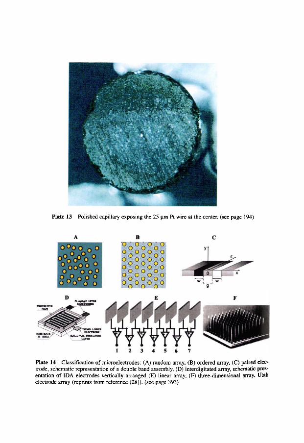
ii
Plate 13 Polished capillary exposing the 25 lam Pt wire at the center. (see page 194)
A B C
0 O 0 0 • 4
• • | • • •
• • • • • q) •
• • • • • •
• • • O q) • • • • • g
D lg t~ , t~t le l ~
It lUl~.," "--2 I d~V~O~ ImUI~TDIC
1 2 3 4 S 6 7
Plate 14 Classification of microelectrodes: (A) random array, (B) ordered array, (C) paired elec- trode, schematic representation of a double band assembly, (D) interdigitated array, schematic pres- entation of IDA electrodes vertically arranged (E) linear array, (F) three-dimensional array, Utah electrode array (reprints from reference (28)). (see page 393)
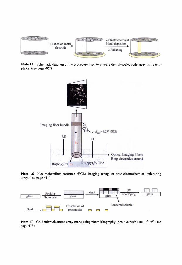
I l.Fixed on metal electrode "-
2.Electrochemical Metal depostion
v
3.Polishing
Plate 15 Schematic diagram of the procedure used to prepare the microelectrode array using tem- plates. (see page 407)
e e
1 . . e
Imaging fiber bundle
RE
Ru(bpy )f*+ i~
A ~ E ~ p p = 1.2V/SCE
CE
I • I
Ru(bpy)33*/TPA
].- Optical Imaging Fibers Ring electrodes around
Plate 16 Electrochemiluminescence (ECL) imaging using an opto-electrochemical microring array. (see page 411 )
uv F-I 1--1 P o s i t i v e t t Mask
glass ] Photoresist glass " developing ~ [-- glass ]
Dissolution of Gold pholoresist I-'! r---!
Rendered soluble 1--I
Plate 17 Gold microelectrode array made using photolithography (positive resin) and lift off. (see page 413)
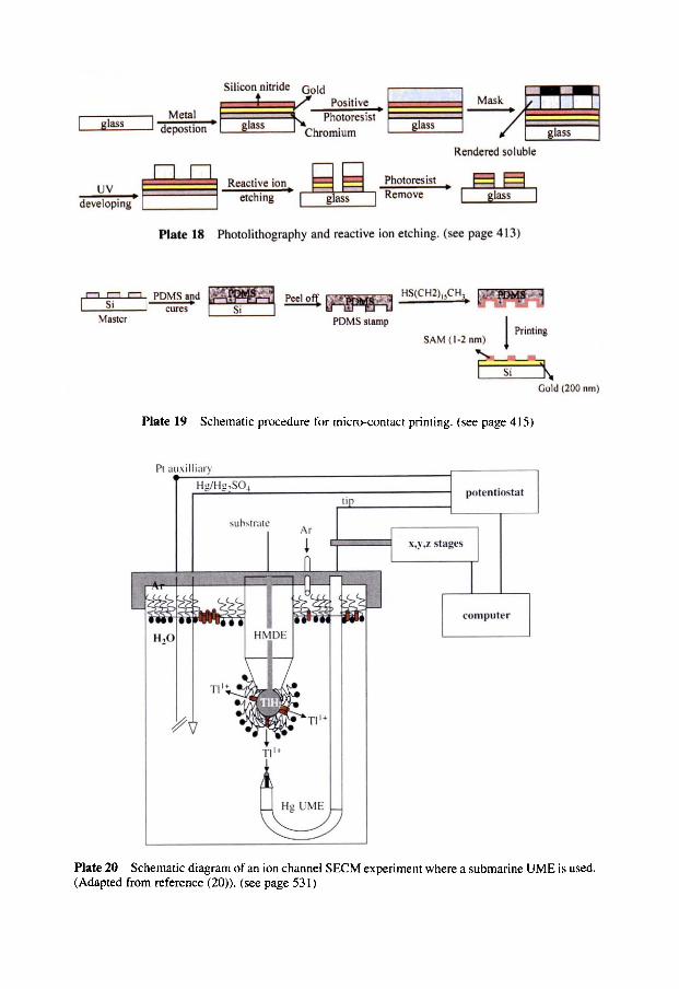
[ glass
Silicon nitride Gold ........... :, ~ : - / P o s i t i v e
Metal . t' glass' ~ . , Pho.toresist I dep°sti°n + ' t.nromtum
UV developing =
• , , , ,
' " g~ss
Mas
Rendered soluble
Reactive ion ~ ~ Photores is t ~ ~ etching I g~+ I R+mov+ i g~a~
Plate 18 Photolithography and reactive ion etching. (see page 413)
[ ~ ~ ~ PDMS and ~ Peel o~ - HS(CH2),sCH3- [ ) ~ ~ ~ : : : i ~ si ~ u ~ , [ s~ i - ~ ' " ~" ~:: ......... ........ i:,
Master PDMS stamp / Printing
SAM (!-2 nm) 1 I F
Gold (200 rim)
Plate 19 Schematic procedure for micro-contact printing. (see page 415)
PI auxilliary
H , O
Hg/Hg2SO_~
suhstrate
tip I
A r :[ +o -:m
6
x,y,z stages
potentiostat
computer
HP
i
i
~11+
+l-l I+
UME _
Plate 20 Schematic diagram of an ion channel SECM experiment where a submarine UME is used. (Adapted from reference (20)). (see page 531)