Embed Size (px)
Citation preview
Eur. J. Solid State lnorg. Chem. t. 35, 1998, p. 211-219
Highly conducting and transparent sprayed indium tin oxide
M. RAMI, E. BENAMAR, C. MESSAOUDI, D. SAYAH and A. ENNAOUI Laboratoire de Physique des Mat6fiaux, Facult6 des Sciences, BP 1014, Rabat, Maroc
(E. K., received February 27, 1998; accepted after revision April 9, 1998.)
A B S T R A C T . - S p r a y pyrolysis process has been used to deposi t h ighly t ransparent and conduct ing films of tin d o p e d ind ium oxide onto glass substrates . The electrical , opt ical and s t ructura l p roper t i e s have been investigated as a function of various deposi t ion parameters namely dopant concentrat ions, t empera tu re and na ture of substrates. X-ray diffract ion patterns have shown that deposi ted films are polycrystall ine without second phases and have preferred orientation [400]. Ind ium tin oxide layers with
small resistivity value around 7.10 -5 ~q.cm and transmission coefficient in the visible and near IR range of about 85-90 % have been easily obtained.
INTRODUCTION Indium tin oxide (ITO) has a wide range of applications in
optoelectronic devices and in solar cells (e.g. by controlling the resistivity, we can use low conductivity ITO as buffer layer and highly conducting ITO as front contact in thin films CuInS2 and CuInSe2 based solar cells) due to its wide band gap (sufficient to be transparent) in both visible and near infrared range, and high
Eur. J. Solid State lnorg. Chem., 0992-4361/98/3/O Elsevier, Paris
212 M. RaMI et al.
carrier concentrations wi th metallic conduction. A variety of deposition techniques such as reactive electron beam evaporation [1], DC magnetron sputtering [2], evaporation [3], reactive thermal deposit ion [4], and spray pyrolysis [5,6] have been used for the preparation of undoped and tin doped ind ium oxide. This latter process which makes possible the prepara t ion of large-area coatings has attracted considerable attention due to its simplicity and large scale wi th low cost fabrication. By scanning the l i t terature, there are m a n y articles d iscuss ing the general propert ies of ITO thin films such as s tructure [7,8], electrical properties [4,9,10] and optical properties [10-12]. The aim of our investigation is to improve the quality of sprayed ITO thin films and to reduce their preparation cost by using low concentrations of the precursors. In this work,we have been able to de termine the experimental condit ions necessary to obtain layers with high conductivity and transparency by measuring the resistivity and the transmission respectively.
EXPERIMENTS Tin doped ind ium oxide was deposited by spraying an alcoholic solution containing ind ium chloride InC13 (Merck, 99,9) and tin chloride SnC14, 5H20 (Aldrich, 98) used as dopant onto glass substrates heated at different temperatures. Hydrochloric acid was added to increase the solubility of the solution. The layers were deposited on two kinds of substrates: pyrex and microscope slide glasses. The optimal deposi t ion parameters of the as-deposited ITO thin films are given in table 1.
TABLE I - Spray conditions.
Indium chloride Ethanol Tin chloride Hydrochloric acid Substrate temperature Carrier gaz Spray rate
0.025 M 25% of solution 0.75- 2 mM 0.05 M 400°C-500°C Air 2.5 roll rain
TOME 35 -- 1998 -- N ° 3
H I G H L Y C O N D U C T I N G A N D T R A N S P A R E N T S P R A Y E D I N D I U M T I N O X I D E 213
All the above ment ioned parameters were kept constant and only the concentration of SnC14 and the substrate temperature were changed. The concentra t ion of SnC14 is expressed in molar concentration relatively to InCl3. An X-Ray diffractometer ( Siemens D5000 ) with Ni-filtred CuKc~ rad ia t ion was used for X-ray dif f ract ion (XRD) s tudies . Microstructural investigations were carried out by using scanning electron microscope (Jeol GSM-T330 ). The dark electrical resistivity was measu red us ing the usual four points probe technique. The Optical transmittance and absorbance of the films were recorded in the wavelength range 0.2 ~tm to 1.1 p m using a Perkin Elmer Lambda 2 UV-VIS spectrophotometer.
~, (a)
(b)
i n II I " •
• J . , i A ~
(c)
(d)
10 20 30 40 50 60
20 (deg)
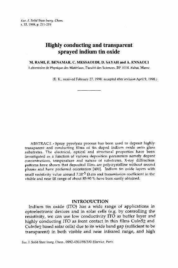
Fig. 1 - X-ray diffraction patterns for ITO films grown on pyrex substrates at different temperatures 400°C (a), 450°C (b), 500°C (c) and grown on glass
microscope slide substrates at 400°C (c).
E U R . J. SOLID S T A T E 1NORG. C H E M .
214 M. RAMI et al.
RESULTS A N D DISCUSSIONS M o r p h o l o g y a nd s t ruc tu re
Acco rd ing to the XRD pa t t e rns (Figure 1) the a s -depos i t ed fi lms g r o w n on to p y r e x glass subst ra tes at t e m p e r a t u r e r ang ing f ro m 400 to 500°C are polycrystalline and exhibit a preferential orientation along the (400) direction corresponding to a cubic structure. The ratio of the (400) and (222) used to evaluate the effect of the temperature on the texture of the films shows that the films p repared at T= 500°C (I400/1222 = 15 ) have the best structure compared to the films prepared at T=450°C (I400/1222 = 7.6 ) and T= 400°C (1400/I222= 5.5 ). No change in the XRD spectra be tween undoped and tin doped indium oxide is observed for the same t empera tu re . The films depos i t ed onto microscope slide show a weaker preferential orientation compared to those grown onto pyrex (compare fig. ld and fig. la). The lattice parameter "a" of the films as determined by XRD data was found to be a = 10.14 /k which is in good agreement with the value given by A.S.T.M table ( American standard of testing materials). Figure 2 shows the scanning micrograph of the surface morphology of an indium tin oxide sprayed on a pyrex substrate at t empera ture
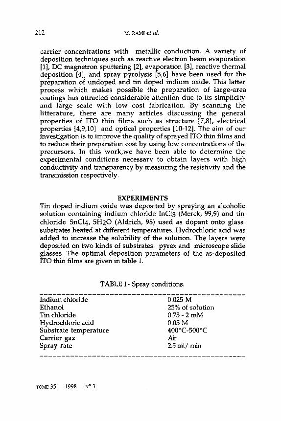
T=500°C with thickness of about l~tm. The films are homogenous and have very small spherical grains.
Fig. 2 - Scanning electron micrograph of ITO thin film sprayed on a pyrex glass substrate at temperature T= 500°C.
TOME 35 - - 1998 - - N ° 3
HIGHLY CONDUCTING AND TRANSPARENT SPRAYED INDIUM TIN OXIDE 215
Electrical properties The electrical conductivity of the ITO films grown on both pyrex
and microscope slide substrates were measured directly by using a Siemens B 1021 mult imeter and a usual four point probe method. Small resistivities were obtained for ITO layers deposi ted onto pyrex substrates with thicknesses varying from 0.4 ~tm to 0.8 ~tm. Table 2 compares our results with some recent published works.
TABLE II - Performance of the resistivity of the ITO thin films.
Synthesis technique Resistivity value (f~.cm) Reference
Sputtering 2 10-4 [2] Evaporat ion 5-6 10 -4 [9] Spray 4 10 -5 in this work Spray 4.8 10 -4 [13]
120
..lO0
40
~ 20
o o,
I I I I I A I T O / m i c r o s e o p e s l i d e
i - Dopant concentration (%)
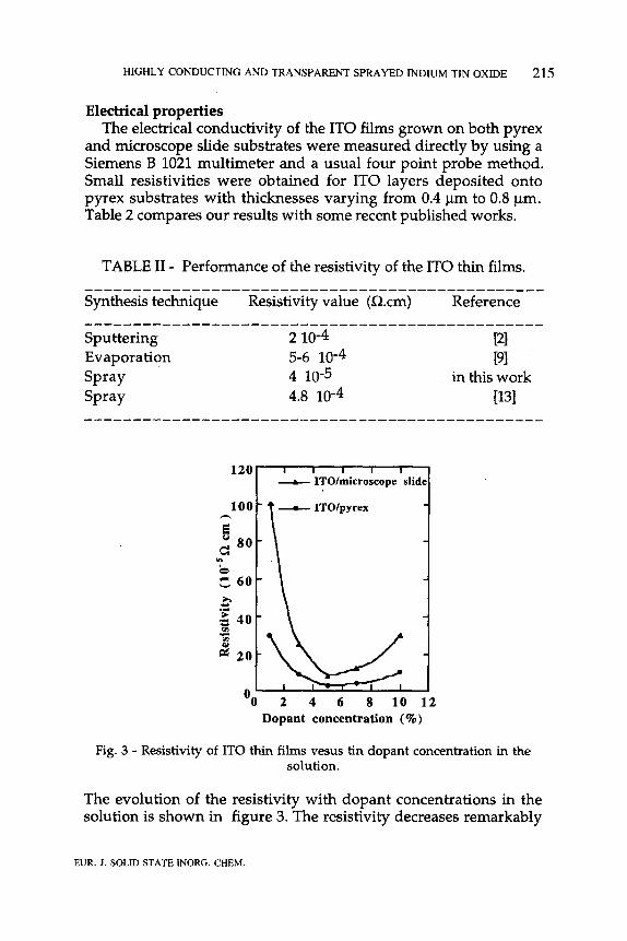
Fig. 3 - Resistivity of ITO thin films vesus tin dopant concentration in the solution.
The evolution of the resistivity with dopant concentrations in the solution is shown in figure 3. The resistivity decreases remarkably
EUR. J. SOLID STATE INORG. CHEM.
216 M. RAM! etal.
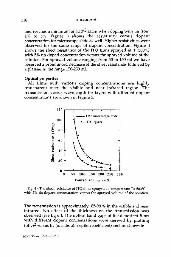
and reaches a min imum of 4.10 -5 ga.cm when doping with tin from 1% to 5%. F igure 3 s h o w s the res i s t iv i ty v e r s u s d o p a n t concentration for microscope slide as well. Higher resistivities were observed for the same range of dopan t concentration. Figure 4 shows the sheet resistance of the ITO films sprayed at T=500°C with 5% tin doped concentration versus the sprayed vo lume of the solution. For sprayed vo lume ranging from 50 to 150 ml we have observed a pronounced decrease of the sheet resistance fol lowed by a plateau in the range 150-250 ml.
O p t i c a l p r o p e r t i e s All fi lms wi th va r ious d o p i n g concen t ra t ions are h igh ly
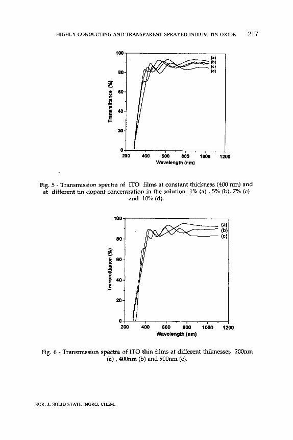
t r ansparen t over the vis ible and near inf rared region. The transmission versus wave length for layers wi th different dopan t concentrations are shown in Figure 5.
° ~
k
120
100
80
60
40
20
0 0
! I I I i
~ I T O / m i c r o s c o p e s l i d e
/ p y r e x
I I I I I
50 100 150 200 250 300
Poured volume (ml)
Fig. 4 - The sheet resistance of ITO films sprayed at temperature T= 500°C with 5% tin dopant concentration versus the sprayed volume of the solution.
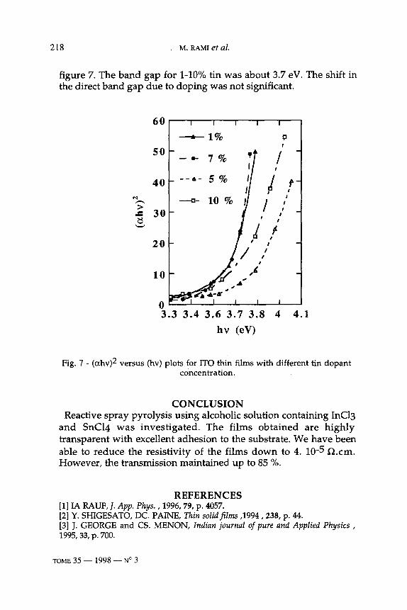
The transmission is approximately 85-90 % in the visible and near infrared. No effect of the thickness on the t ransmiss ion was observed (see fig 6 ). The optical band gaps of the deposi ted films with different d o p a n t concentrat ions were der ived by plot t ing (ahv) 2 versus hv (0¢ is the absorption coefficient) and are shown in
TOME 35 - - 1998 - - N ° 3
HIGHLY CONDUCTING AND TRANSPARENT SPRAYED INDIUM TIN OXIDE 217
100- (a)
/ ~ ~ ( b ) (c)
i
'2t 200 ,~o e;o ~o l&o 12oo
Wavelength (nm)
Fig. 5 - Transmission spectra of ITO films at constant thickness (400 nm) and at different tin dopant concentration in the solution 1% (a), 5% (b), 7% (c)
and 10% (d).
100-
80-
A
so- r ,
J E ~ 4o-
O, 2OO
i
~ (a) (b) (c)
400 600 800 10()0 1200 Wavelength (nm)
Fig. 6 - Transmission spectra of ITO thin films at different thiknesses 200nm (a), 400nm (b) and 900nm (c).
EUR. J. SOLID STATE INORG. CHEM.
218 M. RAMI et al.
f igure 7. The b a n d gap for 1-10% tin was abou t 3.7 eV. The shif t in the direct b a n d gap d u e to d o p i n g was no t significant.
>
6 0 I I I I I
A 1% t
7 i - 40 - - - - 5 % 11 / t- 30- n- 10 % / ~ ] in,,,/ _
2010 -~.//ii '''/' - 0 3.3 3.4 3.6 3.7 3.8 4 4.1
hv (eV)
Fig. 7 - (¢hv) 2 versus (hv) plots for ITO thin films with different tin dopant concentration.
C O N C L U S I O N React ive sp r ay pyro lys i s us ing alcoholic so lu t ion con ta in ing InC13
a n d SnC14 w a s i n v e s t i g a t e d . T h e f i lms o b t a i n e d a re h i g h l y t r anspa ren t w i th excel lent adhes ion to the substrate . W e h av e b een
able to r e d u c e the res i s t iv i ty of the fi lms d o w n to 4. 10-5 gi .cm. H o w e v e r , the t ransmiss ion ma in ta ined up to 85 %.
REFERENCES [1] IA RAUF, J. App. Phys., 1996, 79, p. 4057. [2] Y. SHIGESATO, DC. PAINE, Thin solidfilms ,1994,238, p. 44. [3] J. GEORGE and CS. MENON, Indian journal of pure and Applied Physics, 1995, 33, p. 700.
TOME 35 - - 1998 - - N ° 3
HIGHLY CONDUCTING AND TRANSPARENT SPRAYED INDIUM TIN OXIDE 219
[4] P. THILAKAN, S. KALAINATHAN, J. KUMAR and P. RAMASAMY, Journal of Electronic Materials, 1995, 24 ,p. 719. [5] CH. LEE, CS. HUANG, Materials Science and engineering (-Solid state Materials for Advanced Technology, 1994, 22, p. 233. [6] S. MIRZAPOUR, S. M. ROZATIS, M.G. TAKWALE, B.R. MARATHE and V. G. BHID, Mat. Res. Bull., 1992, 27, p. 1133. [7] IA. RAUF, J. YUAN, Materials Letters, 1995, 25(5-6), p. 217. [8] M. KAMEI, Y. SHIGESTO, S. TAKAKI, Thin solid films, 1995, 259 (1L p.38. [9] S. NOGUSHI, H. SAKATA,Thin solid films, 1988, 157, p. 181. [10] R. G. DHERE, T. A. GESSERT, L. L. SCHILLING, A. J. NELSON, K. M. JONES, H. AHARONI and T. J. Coutts, solar cells, 1987, 21, p. 281. [11] F. DEMICHELIS, E. MINETTI-MEZZETTI, V. SMURRO, A. TAGLIFERRO, and E. TRESSO, J. Phys. D- Appl. Phys. 1995, 18, p. 1825. [12] IA. RAUF, J. Phys. D- Appl. Phys., 1994, 27, p. 1083. [13] J. C. MANIFACIER, L. SZEPESSY, J. F. BRESSE, M. PEROTIN and R. STUCK,Mat. Res. Bull, 1979, 14, p.163.
EUR. J. SOLID STATE INORG. CHEM.


![Investigation of oxide crystals by means of synchrotron ... · X-ray diffraction topography [12 - 24] is a method, which can be effectively used for the characterization of oxide](https://img.pdfslide.fr/doc/110x75/5f643048d97a2737ec6c8884/investigation-of-oxide-crystals-by-means-of-synchrotron-x-ray-diffraction-topography.jpg)