Embed Size (px)
Citation preview
Optical and morphological properties of GaN quantum dots doped with Tm
T. Andreev,1,* Y. Hori,1,2 X. Biquard,1 E. Monroy,1 D. Jalabert,1 A. Farchi,1 M. Tanaka,2
O. Oda,2 Le Si Dang,3 and B. Daudin11CEA/CNRS/UJF research group Nanophysique et Semiconducteurs, 17 rue des Martyrs, 38054-Grenoble cedex 9, France
2NGK Insulators, Ltd., 2-24 Sudacho, Mizuhoku, Nagoya, Japan3CEA/CNRS/UJF research group Nanophysique et Semiconducteurs, Laboratoire Spectrométrie Physique (CNRS UMR5588),
Université J. Fourier, Boîte Postale 87, 38402 Saint Martin d’Hères, FrancesReceived 16 November 2004; published 16 March 2005d
We report on optical and structural properties of wurtzite-phase Tm-doped GaN quantum dotssQDsd em-bedded in an AlN matrix, grown by plasma-assisted molecular beam epitaxy. The influence of Tm on the sizeand shape of the QDs is analyzed. The optical properties are studied using cathodoluminescence and photolu-minescence. Intra-4f-Tm transitions from the1D2 level show constant temperature behavior from 10 K toroom temperature. The internal electric field and strains in the QDs yield a redshift and an additional broad-ening of the lines. We demonstrate that Tm atoms are partially located in the GaN QDs and partially at theGaN/AlN interface.
DOI: 10.1103/PhysRevB.71.115310 PACS numberssd: 78.66.Fd, 68.55.Ln, 85.60.Jb, 68.65.Hb
I. INTRODUCTION
Rare-earthsREd dopants in wide-band-gap semiconduc-tors like III-nitrides lead to sharp intra-4f optical transitionswhich extend from the infrared to the ultraviolet. Efficientenergy transfer from the semiconductor host can take placeonly if the band-gap energy is higher than the energy level ofthe rare-earth atoms. After band-to-band excitation of thehost semiconductor, the generated free electrons can be cap-tured by a RE-related trap. Next an electron-hole pair can beformed, due to Coulomb interactions. A nonradiative recom-bination of the pair leads to the excitation of the RE ion,resulting in the observed luminescence. Thus, doping withEu, Sm, or Prsredd, Er sgreen and infraredd, Tb or Hosgreend, and Tmsblued could provide an alternative solutionfor full-color light-emitting diodes.1–8
The band gap of thesIndGaN host is wide enough to allowRE transitions, in the whole visible range. However, the REradiative quantum efficiency strongly depends on the carrier-mediated energy transfer process, which has to compete withfast nonradiative recombination channels. To overcome thisproblem, we propose to dope GaN or InGaN quantum dotssQDsd with RE ions. Then the carrier-mediated energy trans-fer to the RE should be improved significantly since QDs areparticularly efficient carrier trapping centers. Along theselines, optical properties of Eu-doped GaN QDs embedded inan AlN matrix have been studied, showing that confinementin QDs yields an intense and thermally stable red photolumi-nescencesPLd.9 We also reported that the growth mechanismof GaN nanostructures was drastically affected in the pres-ence of Eu, with strong perturbations of the morphology ofthe QDs.10 Based on structural characterizations, namely, ex-tended x-ray absorption fine structuresEXAFSd and Ruther-ford backscattering spectroscopysRBSd, Eu was found tooccupy the Ga site inside the QDs.9
In the case of Tm doping, blue electroluminescence fromdoped GaN films has already been reported.11–14 However,the PL intensity was found to be much higher in the case of
AlN:Tm layers than in the case of GaN:Tm layers. In par-ticular, transitions from the1D2 level, the most relevant forblue light emission, are not seen in GaN:Tm films.15–18
The charge state of the RE ions is directly reflected in theluminescence. In RE3+ ions, inner-shell transitions are domi-nant. The effect of the surrounding host is weak, yielding tosharp luminescence lines, contrary to the much broader linesfrom RE2+ ions, characterized by outer-shell transitionsssee,for example, Ref. 19d.
The aim of this article is to analyze the effect of Tmdoping on the optical and morphological properties of GaNQDs, and to assess the capability of this rare earth for bluelight emission at room temperature.
The article is organized as follows. First we show how themorphology of the QDs is affected by the presence of Tm.Next, we discuss optical properties, namely, cathodolumines-cencesCLd results on AlN:Tm and GaN:Tm QDs and PLmeasurements, where the temperature dependence of thetransitions can help to assign their origin. We show that thecarrier-mediated energy transfer to the1D2 level is made al-lowed in doped QDs. Moreover the transitions related to thislevel are found to be remarkably stable with respect to thetemperature. Finally, the issue of the exact location of Tmatoms within the GaN/AlN heterostructure is addressed bydiscussing EXAFS and RBS results.
II. EXPERIMENT
All experiments were performed using 1-mm-thick AlNpseudosubstrates deposited by metal organic chemical vapordeposition onc-sapphire.20 After a standard chemical de-greasing procedure and acid cleaning, they were fixed withindium on a molybdenum sample holder, and introduced intoa molecular beam epitaxy chamber equipped with Al, Ga,and Tm effusion cells and a radio-frequency plasma cell toproduce active nitrogen. The GaN QDs were grown at asubstrate temperature of 720 °C following the Stranski-Krastanow growth mode, i.e., the QDs appear after the depo-
PHYSICAL REVIEW B 71, 115310s2005d
1098-0121/2005/71s11d/115310s8d/$23.00 ©2005 The American Physical Society115310-1
sition of a GaN wetting layer of about two monolayerssMLsd.21,22 The growth conditions were controlled with re-flection high-energy electron diffraction, which allowsin situmonitoring of the QD formation. During the growth of GaN,the Tm shutter was opened in order to dope the material.Next, the QDs were capped by about 12 nm of AlN. Thisprocess was repeated several times to achieve superlattices ofQD planes. The last layer of QDs was left uncapped to en-able morphological analysis by atomic force microscopysAFMd. For morphological studies of the QDs, a series ofsamples containing 20 planes with various Tm content wasgrown. A 60-nm-thick AlN:Tm layer and a 200-nm-thickGaN:Tm layer were also grown on an AlN and GaN buffer,respectively, as reference samples for optical experiments.
The Tm mole fraction of the samples was measured byRBS, with a typical uncertainty of ±2%. The Tm contentindicated throughout the paper has been calculated by arbi-trarily assuming that all Tm atoms are located inside theGaN material. In other words, it is important to notice thatRBS provides accurate information on the quantity of Tm inthe superlattice, but lacks in the present case the spatial reso-lution to determine if Tm is incorporated within the GaNQDs or in the AlN spacer.
In order to investigate the exact location of incorporatedTm, EXAFS experiments were performed at beamlineFAME sBM30Bd at the European Synchrotron Radiation Fa-cility in Grenoble. EXAFS spectra were recorded at the TmLIII edges8648 eVd in fluorescence mode with a 30-elementenergy-resolved detector. Experiments were conducted atroom temperature, and the 2503250 mm2 x-ray spot waskept centered during scans by dynamically adjusting the cur-vature of the second crystal of the Sis220d monochromatorand tracking the beam height. Good harmonic rejection andmaximal resolution is achieved thanks to two Rh-coated mir-rors of adjustable tilt and curvature situated on both sides ofthe monochromator. The incidence angle of the x-ray beamon the sample’s surface was kept constant at around 35°.Energy calibration was made using an Al-capped Tm layerdeposited onto a GaN/Al2O3 substrate. Baseline extractionwas done using theAUTOBK program23 and data analysis wasconducted using theFEFF and FEFFIT package programs.24
Before both RBS and EXAFS experiments, the samples werechemically cleaned with HCl in order to remove possiblesegregated Tm atoms from the surface.
Cathodoluminescence was carried out with a FEI Quanta200 SEM equipped with a Jobin Yvon HR460 monochro-mator and charge-coupled device camera operating at liquidnitrogen temperature The injected current was 890 pA at aspot size of 0.2mm. Temperature-dependent PL was mea-sured with the fourth harmonic of a pulsed neodymium-doped yttrium aluminum garnetsNd:YAGd lasers266 nmd,with a pulse width of 0.5 ns, repetition rate of 8 kHz, andaverage excitation power of 4.5 mW. Complementary mea-surements of the infrared signal were performed with the305 nm line of an Ar+ laser. The spot size of the laser wasnonfocused, covering about 2 mm2 of the sample, in order tominimize the effect of drifts during temperature-dependentmeasurements. Even in the case of a well-focused spots,200 mmd we do not observe significant changes in thespectra due to the high dot densities.
III. QUANTUM DOT GROWTH AND MORPHOLOGY
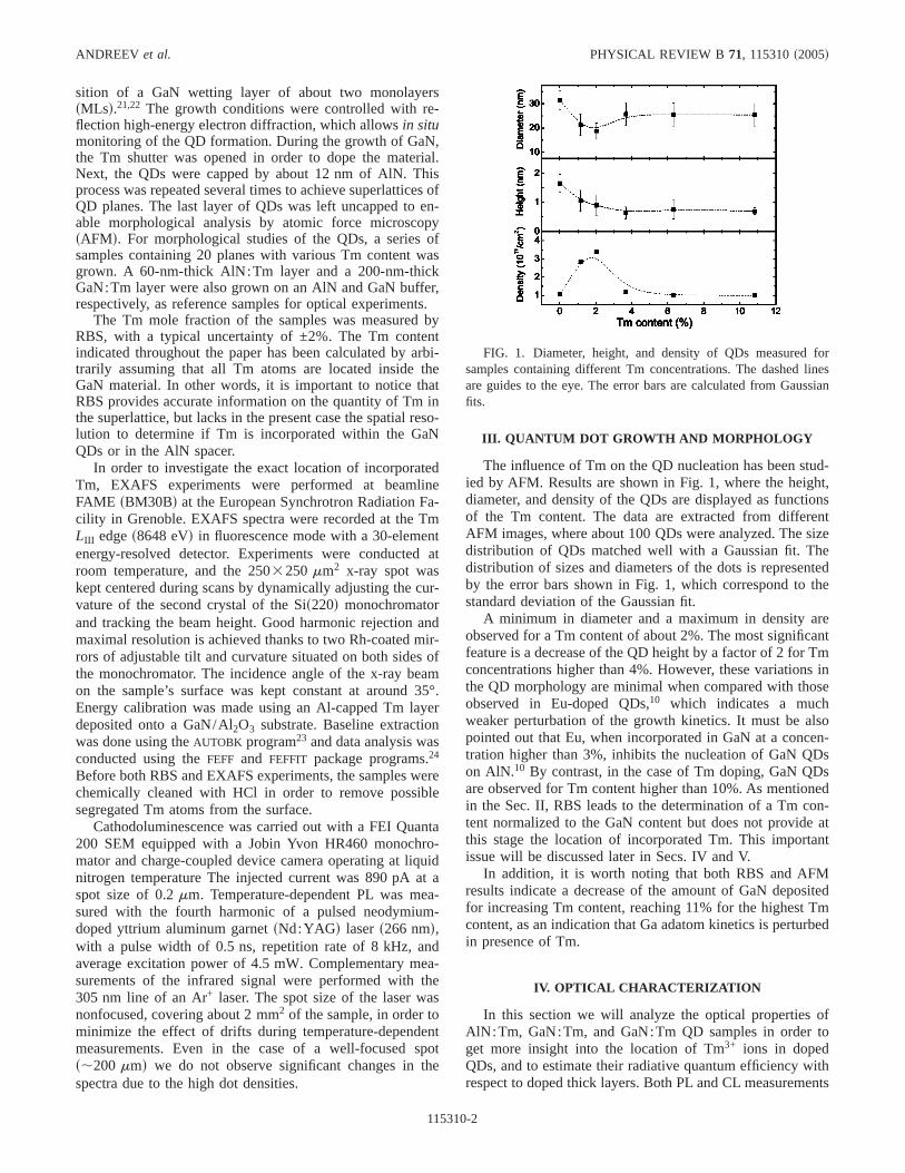
The influence of Tm on the QD nucleation has been stud-ied by AFM. Results are shown in Fig. 1, where the height,diameter, and density of the QDs are displayed as functionsof the Tm content. The data are extracted from differentAFM images, where about 100 QDs were analyzed. The sizedistribution of QDs matched well with a Gaussian fit. Thedistribution of sizes and diameters of the dots is representedby the error bars shown in Fig. 1, which correspond to thestandard deviation of the Gaussian fit.
A minimum in diameter and a maximum in density areobserved for a Tm content of about 2%. The most significantfeature is a decrease of the QD height by a factor of 2 for Tmconcentrations higher than 4%. However, these variations inthe QD morphology are minimal when compared with thoseobserved in Eu-doped QDs,10 which indicates a muchweaker perturbation of the growth kinetics. It must be alsopointed out that Eu, when incorporated in GaN at a concen-tration higher than 3%, inhibits the nucleation of GaN QDson AlN.10 By contrast, in the case of Tm doping, GaN QDsare observed for Tm content higher than 10%. As mentionedin the Sec. II, RBS leads to the determination of a Tm con-tent normalized to the GaN content but does not provide atthis stage the location of incorporated Tm. This importantissue will be discussed later in Secs. IV and V.
In addition, it is worth noting that both RBS and AFMresults indicate a decrease of the amount of GaN depositedfor increasing Tm content, reaching 11% for the highest Tmcontent, as an indication that Ga adatom kinetics is perturbedin presence of Tm.
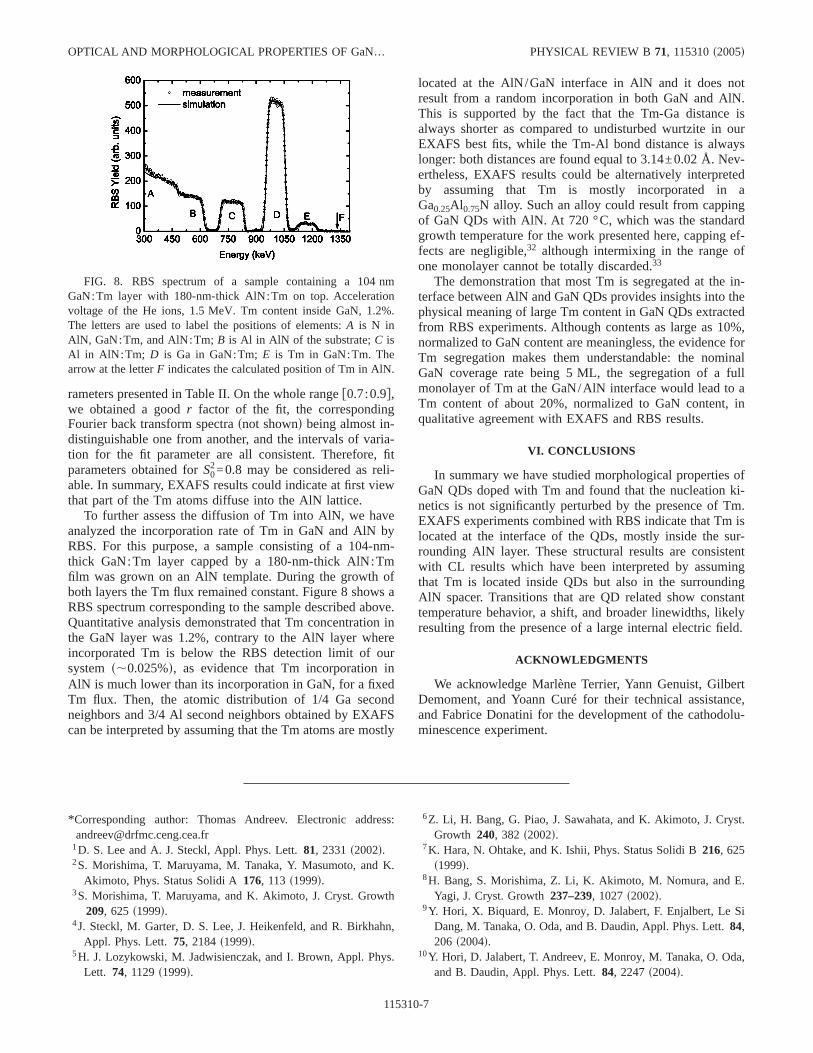
IV. OPTICAL CHARACTERIZATION
In this section we will analyze the optical properties ofAlN:Tm, GaN:Tm, and GaN:Tm QD samples in order toget more insight into the location of Tm3+ ions in dopedQDs, and to estimate their radiative quantum efficiency withrespect to doped thick layers. Both PL and CL measurements
FIG. 1. Diameter, height, and density of QDs measured forsamples containing different Tm concentrations. The dashed linesare guides to the eye. The error bars are calculated from Gaussianfits.
ANDREEV et al. PHYSICAL REVIEW B 71, 115310s2005d
115310-2
have been performed as a function of the temperature. In PL,only energy levels below 4.6 eV can be excited by the fourthharmonic of the Nd:YAG laser. This limiting value corre-sponds to about the energy of the wetting layer of GaN/AlNQD samples, but is smaller than the band gap of AlN.25 ThusPL spectra would mainly display optical transitions fromGaN QDs. By contrast, in CL, the generation volume ofelectrons and holes deeply extends in the sample, typically500 nm s1 mmd deep in a GaNsAlN d layer for a 10 kVelectron beam. As a result, radiative recombinations fromboth GaN QDs and AlN barriers can be observed, whichcould provide complementary information about the locationof Tm ions.
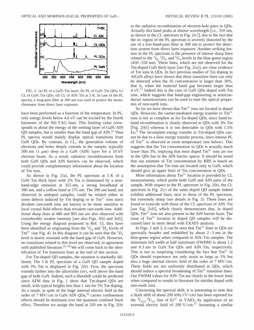
As shown in Fig. 2sad, the PL spectrum at 5 K of aGaN:Tm thick layer with 2% Tm is dominated by a near-band-edge emission at 355 nm, a strong broadband at390 nm, and a yellow band at 575 nm. The 390 nm band, notobserved in undoped samples, could be related either tosome defects induced by Tm doping or to Tm2+ ions sincedivalent rare-earth ions are known to be more sensitive tolocal crystal field effects than trivalent rare-earth ions. Addi-tional sharp lines at 480 and 805 nm are also observed withconsiderably weaker intensityfsee also Figs. 3sbd and 3sddg.Using the energy diagram proposed in Ref. 15, they havebeen identified as originating from the1G4 and3H4 levels ofTm3+ ssee Fig. 4d. In this diagram it can be seen that the1D2level is nearly resonant with the band gap of GaN. However,no transitions related to this level are observed, in agreementwith published literature.15–18We will come back to the iden-tification of Tm transition lines at the end of this section.
For Tm-doped QD samples, the situation is markedly dif-ferent. The 5 K PL spectrum of a GaN QD sample dopedwith 3% Tm is displayed in Fig. 2sbd. First, the spectrumextends further into the ultravioletsuvd, well above the bandgap of bulk GaN. Indeed, such a blueshift could be predictedsince AFM data in Fig. 1 show that Tm-doped QDs aresmall, with typical heights less than 1 nm for 3% Tm doping.As a result, in spite of the huge internal electric field in theorder of 7 MV/cm in GaN/AlN QDs,26 carrier confinementeffects should be dominant over the quantum confined Starkeffect. Therefore we assign the band at 320 nm in Fig. 2sbd
to the radiative recombination of electron-hole pairs in QDs.Actually this band peaks at shorter wavelengthfi.e., 310 nm,as shown in the CL spectrum in Fig. 2scdg, due to the fact thatthe uv region of the PL spectrum is severely distorted by theuse of a low-band-pass filter at 300 nm to protect the detec-tion system from direct laser exposure. Another striking fea-ture in the PL spectrum is the presence of intense sharp linesrelated to the1I6,
1D2, and1G4 levels in the blue-green regions450–550 nmd. These lines, which are not observed for theTm-doped GaN thick layerfsee Fig. 2sadg, are clear evidenceof Tm ions in QDs. In fact previous studies of Tm doping inAlGaN alloys have shown that these transition lines can onlybe detected when the Al concentration is larger than 30%,that is, when the material band gap becomes larger than4 eV.17 Indeed this is the case of GaN QDs doped with Tmions, which suggests that band-gap engineering in semicon-ductor nanostructures can be used to tune the optical proper-ties of rare-earth ions.
So far we have shown that Tm3+ ions are located in dopedQDs. However, the carrier-mediated energy transfer to Tm3+
ions is not as complete as for Eu-doped QDs, since band-to-band recombination is clearly observed in QDs with 3% TmfFig. 2sbdg whereas it is not detectable in QDs with 1.5%Eu.9 The incomplete energy transfer in Tm-doped QDs can-not be due to a slow energy transfer process, since intense PLof Tm3+ is observed at room temperaturessee belowd. Thissuggests that the Tm concentration in QDs is actually muchlower than 3%, implying that most doped Tm3+ ions are notin the QDs but in the AlN barrier spacer. It should be notedthat our estimate of Tm concentration by RBS is based onthe assumption that Tm ions are located only in GaN, whichshould give an upper limit of Tm concentration in QDs.
More information about Tm3+ location is provided by CLmeasurements, which probe both GaN and AlN parts of thesample. With respect to the PL spectrum in Fig. 2sbd, the CLspectrum in Fig. 2scd of the same doped QD sample indeedexhibits additional lines, next to those of the PL spectrum,but extremely sharpssee details in Fig. 3d. These lines arefound to coincide with those of the CL spectrum of AlN:Tmfsee Fig. 2sddg, which clearly demonstrates that, in dopedQDs, Tm3+ ions are also present in the AlN barrier layer. Theissue of Tm3+ location in doped QD samples will be dis-cussed later in more detail with EXAFS analysis.
In Figs. 2 and 3, it can be seen that Tm3+ lines in QDs arespectrally broader and redshifted by about 2–3 nm in theblue-green region when compared to AlN:Tm samples. Theminimum full width at half maximumsFWHMd is about 1.2and 0.3 nm in GaN:Tm QDs and AlN:Tm, respectively.This is not so surprising considering the fact that Tm3+ inQDs should experience not only strain as large as 1% butalso a huge internal electric field of the order of 7 MV/cm.These fields are not uniformly distributed in QDs, whichshould induce a spectral broadening of Tm3+ transition lines.Our FWHM values for AlN:Tm are clearly in the lower limitwhen compared to results in literature for nitrides doped withrare-earth ions.
Concerning the spectral shift, it is interesting to note thata Stark shift of about 200 kHz/sV/cmd has been reported forthe 4I15/2-
4F9/2 line of Er3+ in YAlO3 by application of anexternal electric field of 200 V/cm.27 Assuming a similar
FIG. 2. sad PL of a GaN:Tm layer;sbd PL of GaN:Tm QDs;scdCL of GaN:Tm QDs;sdd CL of AlN:Tm at 5 K. In case of the PLspectra, a long-pass filter at 300 nm was used to protect the mono-chromator from direct laser exposure.
OPTICAL AND MORPHOLOGICAL PROPERTIES OF GaN… PHYSICAL REVIEW B 71, 115310s2005d
115310-3
Stark effect, a shift of the order of 0.1 nm would be expectedfor transition lines in the blue in GaN QDs. Although thisrough estimate is smaller by one order of magnitude thanmeasured data, one should keep in mind that electric fields inQDs are on the MV/cm scale, which is 4 orders of magnitudelarger than the external applied field. In such a case, nonlin-ear Stark effects should take place and induce a larger spec-tral shift.
Finally the key issue of radiative quantum efficiency ofdoped QDs has been investigated by measuring the tempera-ture dependence of Tm3+ PL lines, and results are reported inFigs. 5 and 6. Figures 5sad and 5sbd show the spectra at 10and 300 K, where some transition lines become weaker andsome others are completely quenched. As displayed in Fig.5scd, transitions related to the1D2 level are remarkably stablewith respect to the temperature, whereas those related to the1I6 level are thermally unstable, and those related to the3H4and1G4 levels exhibit an intermediate behavior. It should benoted that, even though the3H4 and1G4 levels are deeper inthe band gap than the1D2 level, the carrier-mediated energytransfer is much more efficient to the1D2 level. This obser-vation strongly supports the existence of an energy transfertrap level close to the1D2 level, which will be investigated inthe future by PL excitation spectroscopy.
In Fig. 6, we compare the temperature dependence of the1G4→3H6 Tm3+ transition at 480 nm in a GaN layer and inGaN QDs. The superior radiative quantum efficiency ofdoped QDs is again demonstrated.9 It can be explained bythe high carrier capture cross section of QDs which shouldenhance any carrier-mediated energy transfer to rare-earthions. Thus doped QDs appear to be a particularly attractivedesign structure for light emitters.
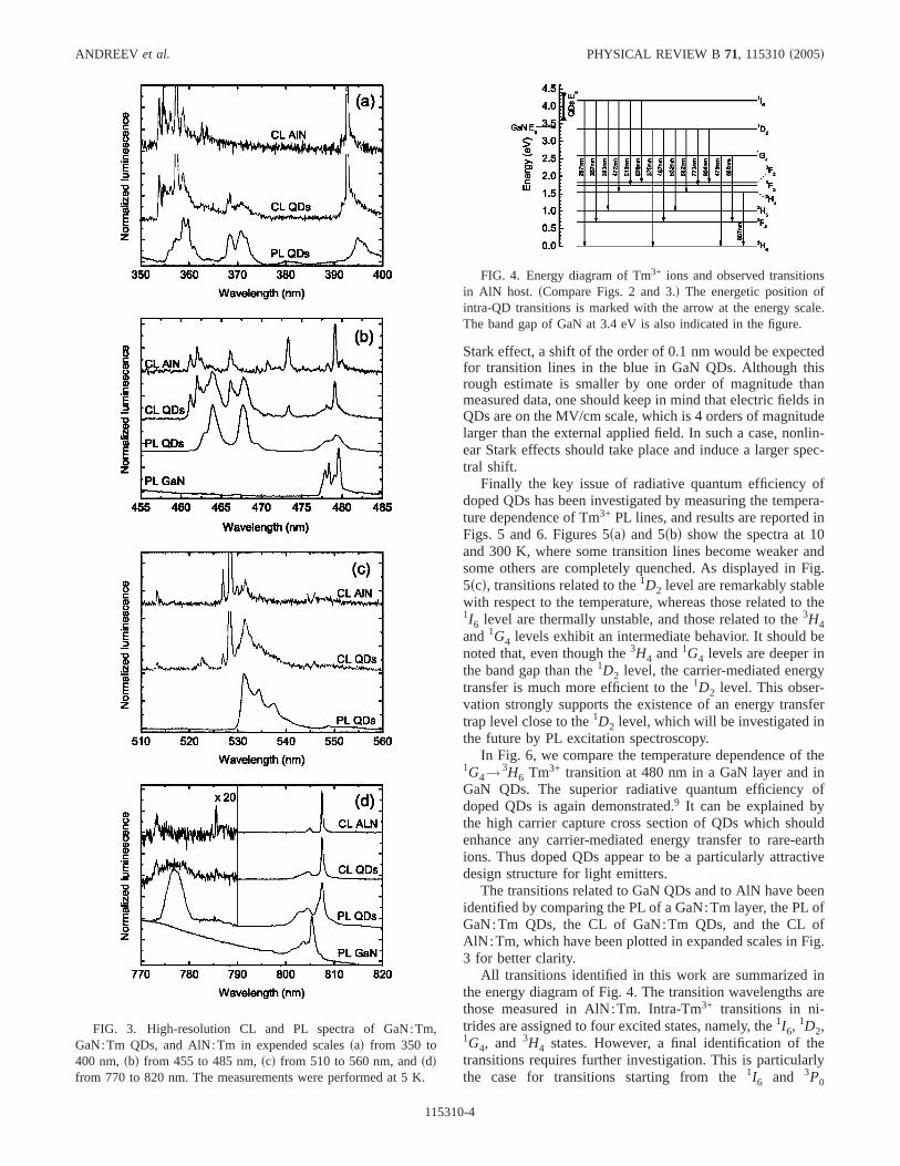
The transitions related to GaN QDs and to AlN have beenidentified by comparing the PL of a GaN:Tm layer, the PL ofGaN:Tm QDs, the CL of GaN:Tm QDs, and the CL ofAlN:Tm, which have been plotted in expanded scales in Fig.3 for better clarity.
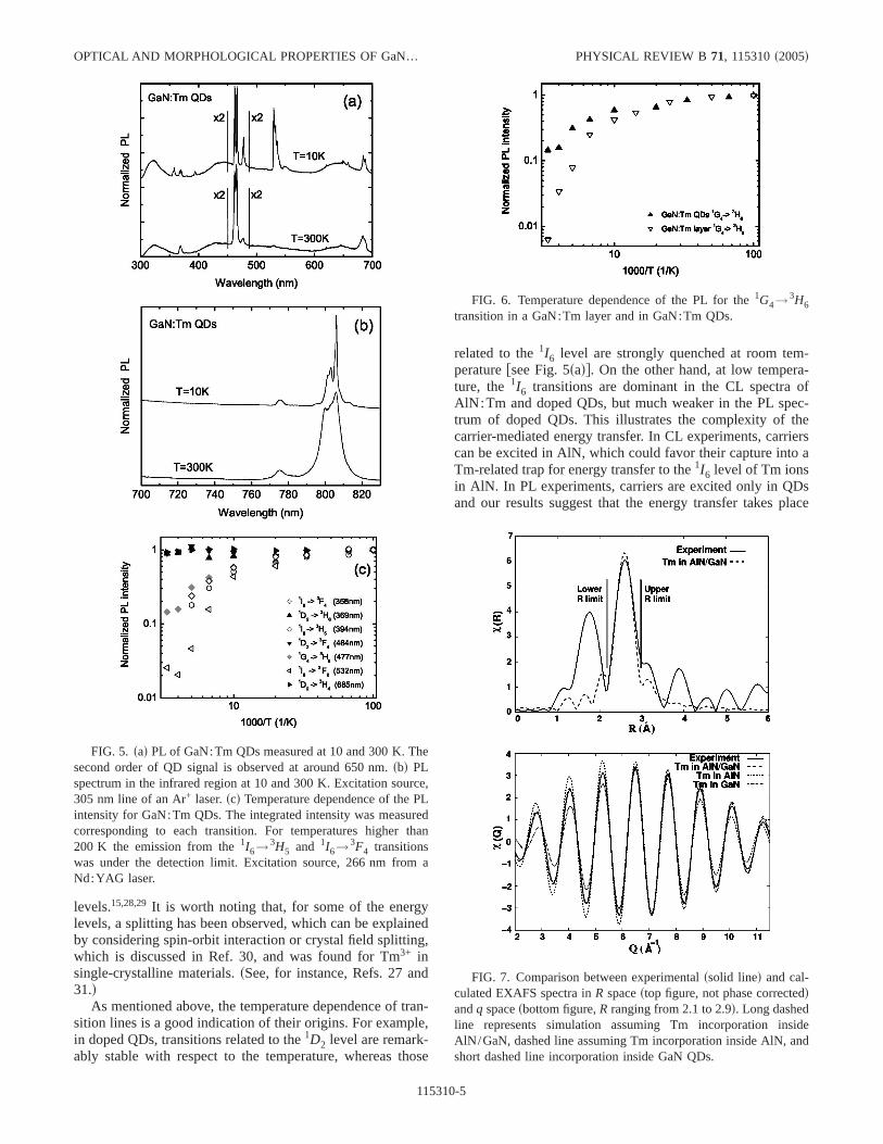
All transitions identified in this work are summarized inthe energy diagram of Fig. 4. The transition wavelengths arethose measured in AlN:Tm. Intra-Tm3+ transitions in ni-trides are assigned to four excited states, namely, the1I6,
1D2,1G4, and 3H4 states. However, a final identification of thetransitions requires further investigation. This is particularlythe case for transitions starting from the1I6 and 3P0
FIG. 4. Energy diagram of Tm3+ ions and observed transitionsin AlN host. sCompare Figs. 2 and 3.d The energetic position ofintra-QD transitions is marked with the arrow at the energy scale.The band gap of GaN at 3.4 eV is also indicated in the figure.
FIG. 3. High-resolution CL and PL spectra of GaN:Tm,GaN:Tm QDs, and AlN:Tm in expended scalessad from 350 to400 nm,sbd from 455 to 485 nm,scd from 510 to 560 nm, andsddfrom 770 to 820 nm. The measurements were performed at 5 K.
ANDREEV et al. PHYSICAL REVIEW B 71, 115310s2005d
115310-4
levels.15,28,29It is worth noting that, for some of the energylevels, a splitting has been observed, which can be explainedby considering spin-orbit interaction or crystal field splitting,which is discussed in Ref. 30, and was found for Tm3+ insingle-crystalline materials.sSee, for instance, Refs. 27 and31.d
As mentioned above, the temperature dependence of tran-sition lines is a good indication of their origins. For example,in doped QDs, transitions related to the1D2 level are remark-ably stable with respect to the temperature, whereas those
related to the1I6 level are strongly quenched at room tem-peraturefsee Fig. 5sadg. On the other hand, at low tempera-ture, the1I6 transitions are dominant in the CL spectra ofAlN:Tm and doped QDs, but much weaker in the PL spec-trum of doped QDs. This illustrates the complexity of thecarrier-mediated energy transfer. In CL experiments, carrierscan be excited in AlN, which could favor their capture into aTm-related trap for energy transfer to the1I6 level of Tm ionsin AlN. In PL experiments, carriers are excited only in QDsand our results suggest that the energy transfer takes place
FIG. 5. sad PL of GaN:Tm QDs measured at 10 and 300 K. Thesecond order of QD signal is observed at around 650 nm.sbd PLspectrum in the infrared region at 10 and 300 K. Excitation source,305 nm line of an Ar+ laser.scd Temperature dependence of the PLintensity for GaN:Tm QDs. The integrated intensity was measuredcorresponding to each transition. For temperatures higher than200 K the emission from the1I6→3H5 and 1I6→3F4 transitionswas under the detection limit. Excitation source, 266 nm from aNd:YAG laser.
FIG. 6. Temperature dependence of the PL for the1G4→3H6transition in a GaN:Tm layer and in GaN:Tm QDs.
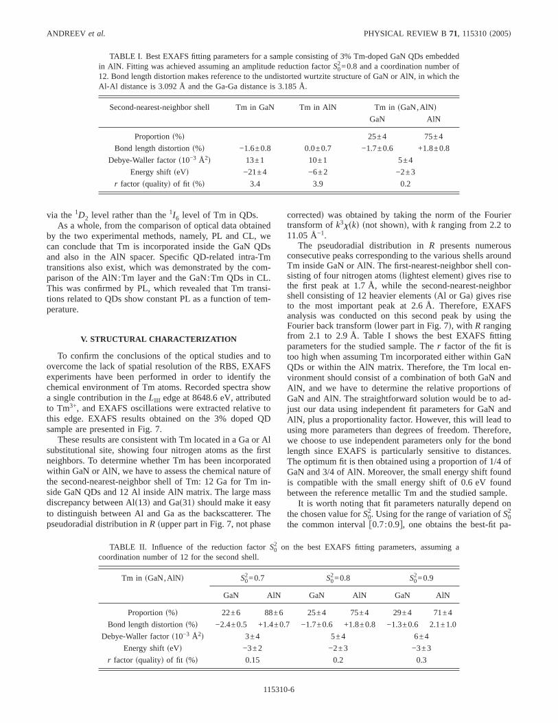
FIG. 7. Comparison between experimentalssolid lined and cal-culated EXAFS spectra inR spacestop figure, not phase correcteddandq spacesbottom figure,R ranging from 2.1 to 2.9d. Long dashedline represents simulation assuming Tm incorporation insideAlN/GaN, dashed line assuming Tm incorporation inside AlN, andshort dashed line incorporation inside GaN QDs.
OPTICAL AND MORPHOLOGICAL PROPERTIES OF GaN… PHYSICAL REVIEW B 71, 115310s2005d
115310-5
via the1D2 level rather than the1I6 level of Tm in QDs.As a whole, from the comparison of optical data obtained
by the two experimental methods, namely, PL and CL, wecan conclude that Tm is incorporated inside the GaN QDsand also in the AlN spacer. Specific QD-related intra-Tmtransitions also exist, which was demonstrated by the com-parison of the AlN:Tm layer and the GaN:Tm QDs in CL.This was confirmed by PL, which revealed that Tm transi-tions related to QDs show constant PL as a function of tem-perature.
V. STRUCTURAL CHARACTERIZATION
To confirm the conclusions of the optical studies and toovercome the lack of spatial resolution of the RBS, EXAFSexperiments have been performed in order to identify thechemical environment of Tm atoms. Recorded spectra showa single contribution in theLIII edge at 8648.6 eV, attributedto Tm3+, and EXAFS oscillations were extracted relative tothis edge. EXAFS results obtained on the 3% doped QDsample are presented in Fig. 7.
These results are consistent with Tm located in a Ga or Alsubstitutional site, showing four nitrogen atoms as the firstneighbors. To determine whether Tm has been incorporatedwithin GaN or AlN, we have to assess the chemical nature ofthe second-nearest-neighbor shell of Tm: 12 Ga for Tm in-side GaN QDs and 12 Al inside AlN matrix. The large massdiscrepancy between Als13d and Gas31d should make it easyto distinguish between Al and Ga as the backscatterer. Thepseudoradial distribution inR supper part in Fig. 7, not phase
correctedd was obtained by taking the norm of the Fouriertransform ofk3xskd snot shownd, with k ranging from 2.2 to11.05 Å−1.
The pseudoradial distribution inR presents numerousconsecutive peaks corresponding to the various shells aroundTm inside GaN or AlN. The first-nearest-neighbor shell con-sisting of four nitrogen atomsslightest elementd gives rise tothe first peak at 1.7 Å, while the second-nearest-neighborshell consisting of 12 heavier elementssAl or Gad gives riseto the most important peak at 2.6 Å. Therefore, EXAFSanalysis was conducted on this second peak by using theFourier back transformslower part in Fig. 7d, with R rangingfrom 2.1 to 2.9 Å. Table I shows the best EXAFS fittingparameters for the studied sample. Ther factor of the fit istoo high when assuming Tm incorporated either within GaNQDs or within the AlN matrix. Therefore, the Tm local en-vironment should consist of a combination of both GaN andAlN, and we have to determine the relative proportions ofGaN and AlN. The straightforward solution would be to ad-just our data using independent fit parameters for GaN andAlN, plus a proportionality factor. However, this will lead tousing more parameters than degrees of freedom. Therefore,we choose to use independent parameters only for the bondlength since EXAFS is particularly sensitive to distances.The optimum fit is then obtained using a proportion of 1/4 ofGaN and 3/4 of AlN. Moreover, the small energy shift foundis compatible with the small energy shift of 0.6 eV foundbetween the reference metallic Tm and the studied sample.
It is worth noting that fit parameters naturally depend onthe chosen value forS0
2. Using for the range of variation ofS02
the common intervalf0.7:0.9g, one obtains the best-fit pa-
TABLE II. Influence of the reduction factorS02 on the best EXAFS fitting parameters, assuming a
coordination number of 12 for the second shell.
Tm in sGaN,AlNd S02=0.7 S0
2=0.8 S02=0.9
GaN AlN GaN AlN GaN AlN
Proportions%d 22±6 88±6 25±4 75±4 29±4 71±4
Bond length distortions%d −2.4±0.5 +1.4±0.7 −1.7±0.6 +1.8±0.8 −1.3±0.6 2.1±1.0
Debye-Waller factors10−3 Å2d 3±4 5±4 6±4
Energy shiftseVd −3±2 −2±3 −3±3
r factor squalityd of fit s%d 0.15 0.2 0.3
TABLE I. Best EXAFS fitting parameters for a sample consisting of 3% Tm-doped GaN QDs embeddedin AlN. Fitting was achieved assuming an amplitude reduction factorS0
2=0.8 and a coordination number of12. Bond length distortion makes reference to the undistorted wurtzite structure of GaN or AlN, in which theAl-Al distance is 3.092 Å and the Ga-Ga distance is 3.185 Å.
Second-nearest-neighbor shell Tm in GaN Tm in AlN Tm insGaN,AlNdGaN AlN
Proportions%d 25±4 75±4
Bond length distortions%d −1.6±0.8 0.0±0.7 −1.7±0.6 +1.8±0.8
Debye-Waller factors10−3 Å2d 13±1 10±1 5±4
Energy shiftseVd −21±4 −6±2 −2±3
r factor squalityd of fit s%d 3.4 3.9 0.2
ANDREEV et al. PHYSICAL REVIEW B 71, 115310s2005d
115310-6
rameters presented in Table II. On the whole rangef0.7:0.9g,we obtained a goodr factor of the fit, the correspondingFourier back transform spectrasnot shownd being almost in-distinguishable one from another, and the intervals of varia-tion for the fit parameter are all consistent. Therefore, fitparameters obtained forS0
2=0.8 may be considered as reli-able. In summary, EXAFS results could indicate at first viewthat part of the Tm atoms diffuse into the AlN lattice.
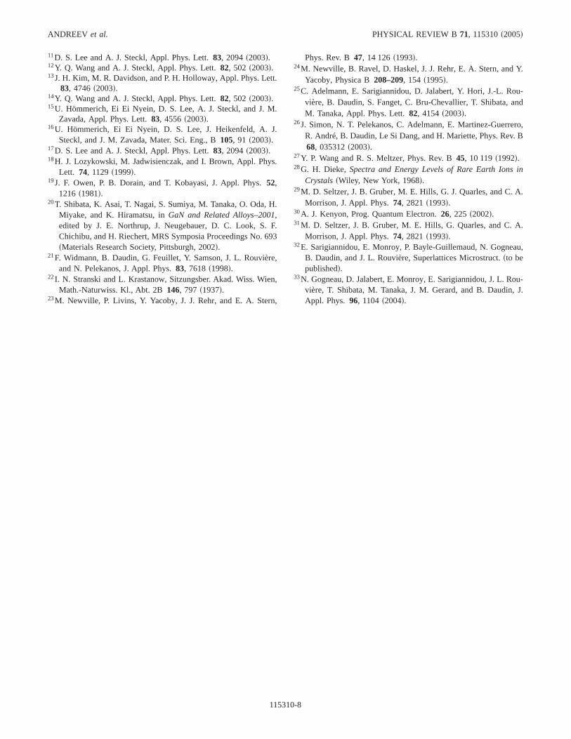
To further assess the diffusion of Tm into AlN, we haveanalyzed the incorporation rate of Tm in GaN and AlN byRBS. For this purpose, a sample consisting of a 104-nm-thick GaN:Tm layer capped by a 180-nm-thick AlN:Tmfilm was grown on an AlN template. During the growth ofboth layers the Tm flux remained constant. Figure 8 shows aRBS spectrum corresponding to the sample described above.Quantitative analysis demonstrated that Tm concentration inthe GaN layer was 1.2%, contrary to the AlN layer whereincorporated Tm is below the RBS detection limit of oursystem s,0.025%d, as evidence that Tm incorporation inAlN is much lower than its incorporation in GaN, for a fixedTm flux. Then, the atomic distribution of 1/4 Ga secondneighbors and 3/4 Al second neighbors obtained by EXAFScan be interpreted by assuming that the Tm atoms are mostly
located at the AlN/GaN interface in AlN and it does notresult from a random incorporation in both GaN and AlN.This is supported by the fact that the Tm-Ga distance isalways shorter as compared to undisturbed wurtzite in ourEXAFS best fits, while the Tm-Al bond distance is alwayslonger: both distances are found equal to 3.14±0.02 Å. Nev-ertheless, EXAFS results could be alternatively interpretedby assuming that Tm is mostly incorporated in aGa0.25Al0.75N alloy. Such an alloy could result from cappingof GaN QDs with AlN. At 720 °C, which was the standardgrowth temperature for the work presented here, capping ef-fects are negligible,32 although intermixing in the range ofone monolayer cannot be totally discarded.33
The demonstration that most Tm is segregated at the in-terface between AlN and GaN QDs provides insights into thephysical meaning of large Tm content in GaN QDs extractedfrom RBS experiments. Although contents as large as 10%,normalized to GaN content are meaningless, the evidence forTm segregation makes them understandable: the nominalGaN coverage rate being 5 ML, the segregation of a fullmonolayer of Tm at the GaN/AlN interface would lead to aTm content of about 20%, normalized to GaN content, inqualitative agreement with EXAFS and RBS results.
VI. CONCLUSIONS
In summary we have studied morphological properties ofGaN QDs doped with Tm and found that the nucleation ki-netics is not significantly perturbed by the presence of Tm.EXAFS experiments combined with RBS indicate that Tm islocated at the interface of the QDs, mostly inside the sur-rounding AlN layer. These structural results are consistentwith CL results which have been interpreted by assumingthat Tm is located inside QDs but also in the surroundingAlN spacer. Transitions that are QD related show constanttemperature behavior, a shift, and broader linewidths, likelyresulting from the presence of a large internal electric field.
ACKNOWLEDGMENTS
We acknowledge Marlène Terrier, Yann Genuist, GilbertDemoment, and Yoann Curé for their technical assistance,and Fabrice Donatini for the development of the cathodolu-minescence experiment.
*Corresponding author: Thomas Andreev. Electronic address:[email protected]
1D. S. Lee and A. J. Steckl, Appl. Phys. Lett.81, 2331s2002d.2S. Morishima, T. Maruyama, M. Tanaka, Y. Masumoto, and K.
Akimoto, Phys. Status Solidi A176, 113 s1999d.3S. Morishima, T. Maruyama, and K. Akimoto, J. Cryst. Growth
209, 625 s1999d.4J. Steckl, M. Garter, D. S. Lee, J. Heikenfeld, and R. Birkhahn,
Appl. Phys. Lett.75, 2184s1999d.5H. J. Lozykowski, M. Jadwisienczak, and I. Brown, Appl. Phys.
Lett. 74, 1129s1999d.
6Z. Li, H. Bang, G. Piao, J. Sawahata, and K. Akimoto, J. Cryst.Growth 240, 382 s2002d.
7K. Hara, N. Ohtake, and K. Ishii, Phys. Status Solidi B216, 625s1999d.
8H. Bang, S. Morishima, Z. Li, K. Akimoto, M. Nomura, and E.Yagi, J. Cryst. Growth237–239, 1027s2002d.
9Y. Hori, X. Biquard, E. Monroy, D. Jalabert, F. Enjalbert, Le SiDang, M. Tanaka, O. Oda, and B. Daudin, Appl. Phys. Lett.84,206 s2004d.
10Y. Hori, D. Jalabert, T. Andreev, E. Monroy, M. Tanaka, O. Oda,and B. Daudin, Appl. Phys. Lett.84, 2247s2004d.
FIG. 8. RBS spectrum of a sample containing a 104 nmGaN:Tm layer with 180-nm-thick AlN:Tm on top. Accelerationvoltage of the He ions, 1.5 MeV. Tm content inside GaN, 1.2%.The letters are used to label the positions of elements:A is N inAlN, GaN:Tm, and AlN:Tm;B is Al in AlN of the substrate;C isAl in AlN:Tm; D is Ga in GaN:Tm;E is Tm in GaN:Tm. Thearrow at the letterF indicates the calculated position of Tm in AlN.
OPTICAL AND MORPHOLOGICAL PROPERTIES OF GaN… PHYSICAL REVIEW B 71, 115310s2005d
115310-7
11D. S. Lee and A. J. Steckl, Appl. Phys. Lett.83, 2094s2003d.12Y. Q. Wang and A. J. Steckl, Appl. Phys. Lett.82, 502 s2003d.13J. H. Kim, M. R. Davidson, and P. H. Holloway, Appl. Phys. Lett.
83, 4746s2003d.14Y. Q. Wang and A. J. Steckl, Appl. Phys. Lett.82, 502 s2003d.15U. Hömmerich, Ei Ei Nyein, D. S. Lee, A. J. Steckl, and J. M.
Zavada, Appl. Phys. Lett.83, 4556s2003d.16U. Hömmerich, Ei Ei Nyein, D. S. Lee, J. Heikenfeld, A. J.
Steckl, and J. M. Zavada, Mater. Sci. Eng., B105, 91 s2003d.17D. S. Lee and A. J. Steckl, Appl. Phys. Lett.83, 2094s2003d.18H. J. Lozykowski, M. Jadwisienczak, and I. Brown, Appl. Phys.
Lett. 74, 1129s1999d.19J. F. Owen, P. B. Dorain, and T. Kobayasi, J. Appl. Phys.52,
1216 s1981d.20T. Shibata, K. Asai, T. Nagai, S. Sumiya, M. Tanaka, O. Oda, H.
Miyake, and K. Hiramatsu, inGaN and Related Alloys–2001,edited by J. E. Northrup, J. Neugebauer, D. C. Look, S. F.Chichibu, and H. Riechert, MRS Symposia Proceedings No. 693sMaterials Research Society, Pittsburgh, 2002d.
21F. Widmann, B. Daudin, G. Feuillet, Y. Samson, J. L. Rouvière,and N. Pelekanos, J. Appl. Phys.83, 7618s1998d.
22I. N. Stranski and L. Krastanow, Sitzungsber. Akad. Wiss. Wien,Math.-Naturwiss. Kl., Abt. 2B146, 797 s1937d.
23M. Newville, P. Livins, Y. Yacoby, J. J. Rehr, and E. A. Stern,
Phys. Rev. B47, 14 126s1993d.24M. Newville, B. Ravel, D. Haskel, J. J. Rehr, E. A. Stern, and Y.
Yacoby, Physica B208–209, 154 s1995d.25C. Adelmann, E. Sarigiannidou, D. Jalabert, Y. Hori, J.-L. Rou-
vière, B. Daudin, S. Fanget, C. Bru-Chevallier, T. Shibata, andM. Tanaka, Appl. Phys. Lett.82, 4154s2003d.
26J. Simon, N. T. Pelekanos, C. Adelmann, E. Martinez-Guerrero,R. André, B. Daudin, Le Si Dang, and H. Mariette, Phys. Rev. B68, 035312s2003d.
27Y. P. Wang and R. S. Meltzer, Phys. Rev. B45, 10 119s1992d.28G. H. Dieke,Spectra and Energy Levels of Rare Earth Ions in
CrystalssWiley, New York, 1968d.29M. D. Seltzer, J. B. Gruber, M. E. Hills, G. J. Quarles, and C. A.
Morrison, J. Appl. Phys.74, 2821s1993d.30A. J. Kenyon, Prog. Quantum Electron.26, 225 s2002d.31M. D. Seltzer, J. B. Gruber, M. E. Hills, G. Quarles, and C. A.
Morrison, J. Appl. Phys.74, 2821s1993d.32E. Sarigiannidou, E. Monroy, P. Bayle-Guillemaud, N. Gogneau,
B. Daudin, and J. L. Rouvière, Superlattices Microstruct.sto bepublishedd.
33N. Gogneau, D. Jalabert, E. Monroy, E. Sarigiannidou, J. L. Rou-vière, T. Shibata, M. Tanaka, J. M. Gerard, and B. Daudin, J.Appl. Phys. 96, 1104s2004d.
ANDREEV et al. PHYSICAL REVIEW B 71, 115310s2005d
115310-8