Embed Size (px)
Citation preview
Short Range Plasmon ResonatorsProbed by Photoemission ElectronMicroscopyLudovic Douillard,* Fabrice Charra, and Zbigniew Korczak†
Commissariat à l’Energie Atomique Saclay Direction des Sciences de la Matière -Institut Rayonnement Matière de Saclay - SerVice de Physique et Chimie des Surfaceset Interfaces, F-91191 Gif sur YVette, France
Renaud Bachelot, Sergei Kostcheev, Gilles Lerondel, Pierre-Michel Adam, andPascal Royer
Laboratoire de Nanotechnologie et d’Instrumentation Optique, ICD CNRS FRE 2848,UniVersité de Technologie de Troyes, 12 rue Marie-Curie, BP 2060,
F-10010 Troyes, France
Received January 8, 2008; Revised Manuscript Received January 29, 2008
ABSTRACT
Short range surface plasmon resonators are investigated at the nanometer scale. Gold nanorods (30 nm in diameter) were microfabricated andprobed by photoemission electron microscopy under direct laser light excitation. Resonances presenting various numbers of lobes occur forspecific rod lengths. A simple analytical model shows that the successive resonant lengths differ by a multiple of one-half of the wavelengthof the supported short-range surface plasmon polariton.
The integration of optics into ever smaller devices ishampered by the long standing barrier of the diffraction limit,namely, the impossibility to confine light below its naturalwavelength, i.e., λ0 in free space or λ0/n in a material ofrefractive index n. In parallel, solid state physics, makinguse of electrons, allows for high integration densities at theexpense of low-band-pass devices. Surface plasmon polari-tons (SPPs) are electromagnetic surface waves coupled tofree electrons at metal dielectric interfaces. As electromag-netic waves, they share the same high working frequency aslight; using free electrons as supporting particles they allowfor spatial confinements over distances smaller than thewavelength of light. So surface plasmon polariton wavesoffer a unique opportunity for scaling down photonic devicesto the nanometer range.1
Among the most traditional electromagnetic devices,antennas,2–4 by converting free-space electromagnetic radia-tion into localized ones, would be especially interesting tobe scaled to nanometer dimensions and optical frequencies.In the radio frequency regime, simple antennas consist in
metal resonators, such as rods whose lengths L are in simplerelation to the incoming or outcoming free radiation wave-length λ0. As the frequency approaches optical regime, andthe rod diameter approaches the material skin depth, SPPdispersion relation departs from the line of light. Indeedinteractions between SPPs propagating along the rod wallsgive rise to coupled modes, known as short-range surfaceplasmon polaritons (SR-SPPs).5,6 The resonance frequenciesare then dictated by the significantly shorter SR-SPPwavelength λSR-SPP, whose value depends on the geometryand material properties.5–10 This further confines the opticalfields around the rod but also introduces severe phase-matching conditions for the resonant mode excitation by freespace waves with natural wavelength λ0 > λSR-SPP.
In this article, we investigate short-range surfaceplasmon polariton resonators at the nanometer scale byphotoemission electron microscopy (PEEM).11–16 In par-ticular, we directly observed coupled plasmonic modes onAu nanorods 30 nm in diameter. By adapting antenna theory,a simple analytical model is derived, enabling the interpreta-tion of rod resonances at optical frequencies. Compared torecent studies by optical microscopy,7,17–19 scanning near fieldmicroscopy (SNOM)20,21 and photoemission electron mi-croscopy15 dealing with noninteracting SPPs excited in
* Corresponding author. E-mail: [email protected].† Permanent address Institute of Physics and Nanotechnology Center,
Maria Curie-Skłodowska University, Pl. M. Curie-Skłodowskiej 1, P-20031Lublin, Poland.
NANOLETTERS
2008Vol. 8, No. 3
935-940
10.1021/nl080053v CCC: $40.75 2008 American Chemical SocietyPublished on Web 02/21/2008
(sub)micrometer objects, the present work addresses thecoupled nature of the plasmonic waves inherited from thedrastic reduction of object sizes. While SR-SPPs are calledto play an important role into the ever smaller photonicdevices, the plasmonics of metal objects of characteristicsections below the evanescent field decay length is largelyunexplored.
Single Au nanorods of length L have been microfabricatedby electron-beam lithography. The rod lengths sample theinterval (50-925 nm) in steps of 25 nm. The rod crosssection is rectangular, 35 nm in height and 30 nm in width.Objects are distributed according to a 6 × 6 matrix and are10 µm distance apart. The whole array size is a square of80 µm length in side. In parallel long rods of length L up to4 µm have been prepared. Size and shape of individualobjects deviate from their expected values by less than 10%as estimated from scanning electron microscopy (SEM). Thesubstrate consists of a 95 nm thick indium tin oxide (ITO)coated silica glass.
The excitation light source used for PEEM measurementsis a continuous wave (CW) mode-locked Ti:sapphire lasersystem (Tsunami, Spectra Physics Inc.) delivering IR photonsin the 740–880 nm range (1.675-1.41 eV). The pulserepetition rate is fixed at 80 MHz. Each pulse exhibits aprofile of 80 fs duration. Two different angles of beamincidence are used, namely, R ) 0° and 75° (90° and 15°with respect to the surface plane). At normal incidence (R) 0°) the light is focused onto the sample through a 500mm focal length lens yielding a circular spot of 730 µm indiameter. At grazing incidence (R ) 75°), a 200 mm focallength lens is used and the spot is an elongated ellipse whoseminor and major axes amount to 260 µm × 1160 µm. Thepeak power densities delivered at the sample surface are inthe range 50-150 MW/cm2. The p-polarization state isselected by a half-wave plate.
The photoemission electron microscope used is a com-mercial instrument (Elmitec GmbH LEEM\PEEM III) op-erating in ultrahigh vacuum at pressure in the low range of10-10 mbar. Lateral spatial resolutions of 10 and 25 nm areroutinely achieved in low-energy electron diffraction (LEEM)and photoelectron emission (PEEM) imaging modes, respec-tively.22 The instrument operates in total electron yield (noenergy filtering).23 The real-space images are recorded via acharge-coupled device (CCD) camera and digitized forfurther analysis (Argus 20, Hamamatsu Inc.). In PEEMimaging mode, the measured brightness in a given imagearea is proportional to the electron emission from that area.Integrated PEEM signal is computed in two steps: (i)background subtraction, i.e., removing of a regression plane,(ii) integration of the pixel values over a representative imagearea. The work function of amorphous Au is in the 4.6-5.1eV range, and no direct one photoemission is expected. Wemeasured that the PEEM signal is proportional to the cubedincident intensity, so the electron emission has its origin ina three-photon absorption process. The collected electronemission reflects the optical near field at the surface ofmetallic nanoobjects. Compared to optical microscopy,7,17–19
scanning field optical microscopy (SNOM)20,21,24, and elec-
tron excitation based techniques,25,26 the photoemissionelectron microscopy permits nanoscale analysis of singlemetal objects under direct laser light illumination. Moredetails about the PEEM experiment can be found in ref 14.
The realization of plasmon-based resonators working inthe optical frequency regime is based on the guidingcapabilities of metal nanowire of subwavelength crosssections.21 For sectional radii R comparable with the skindepth of the metal, the rod walls support coupled plasmonpolariton modes. As previously discussed, the coupled modewe are interested in corresponds to the short-range SPPwaves.5,6 Being efficiently reflected at rod ends, SR-SPPwaves are likely to give birth to strong resonance effects forspecific rod lengths. In addition, SR-SPP waves allow forstrong field confinement at the expense of important propa-gation losses, a latter aspect directly exploited by thephotoemission electron microscopy for object imaging.Quantitatively, at 800 nm excitation wavelength, a SPPpropagating along a single Au/vacuum interface possessesan evanescent field decay length of 25 nm on the metal side.The sectional radii of the microfabricated nanorods are inthe range 30-35 nm and so fulfill the dimensional require-ment for strong coupling leading to SR-SPP excitation.
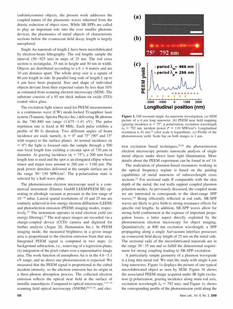
A particularly simple geometry of a plasmon waveguideis a long thin metal rod. We start the study with single 4 µmlong nanowires. Figure 1a displays the picture of one typicalmicrofabricated object as seen by SEM. Figure 1b showsthe associated PEEM image acquired under IR light excita-tion (p polarization, grazing incidence along main rod axis,excitation wavelength λ0 ) 792 nm), and Figure 1c showsthe corresponding profile of the photoemission yield along the
Figure 1. Off-resonant single Au nanowire investigation. (a) SEMpicture of a 4 µm long nanowire. (b) PEEM near field mapping(grazing incidence R ) 75°, p polarization, excitation wavelengthλ0 ) 792 nm, incident power P ) 110 MW/cm2). Longitudinalresolution is 41 nm;19 color scale is logarithmic. (c) Profile of thephotoemission yield. Scale bar on both images is 1 µm.
936 Nano Lett., Vol. 8, No. 3, 2008
wire axis. The propagation of the plasma waves along thenanowire is readily evidenced through the establishment ofstanding-wave patterns at both edges. The PEEM signaloscillates with a period λm ) 466 nm at the leading edgewhile the measured period at the opposite right edge isshorter and amounts to λp ) 256 nm. The peaks in the500–1000 nm region of the photoemission profile presentan unexpectedly high intensity. This phenomenon, notaffecting peak positions, is tentatively attributed to topo-graphic peculiarities.
The observed interference pattern can be rationalized byconsidering the propagation of longitudinal electron chargeoscillations along a one-dimensional conductor under fullfield excitation. The 1D Helmholtz wave equation withexcitation and damping terms is
∂t2F)V�
2∂x
2F+ 1τ∂tF+
qE0
mqei(ωt-k|x) (1)
where F represents the amplitude of the charge displacementfrom equilibrium along the wire axis x, V� the phase velocityof the longitudinal coupled plasma wave, τ its lifetime, andE0ei(ωt-k|x) the distributed CW exciting field acting on chargeq of mass mq. F has the dimension of a length and accountsfor the amplitude of the surface plasma oscillations. Thesecoherent charge fluctuations are accompanied by a mixedtransversal and longitudinal electromagnetic field. Thestationary solutions of eq 1 have the general form
F(x, t)) (Ape+iKx + Ame-iKx -
qE0 ⁄ mq
V�2(K2 - k|
2)e-ik|x)eiωt (2)
with K ) ((ω2 - iω/τ)/V�2)1/2. They consist of two coun-
terpropagating plasmonic free waves with complex wavevec-tors (K (K ) K1 + iK2 with K1 and K2 real), superimposedto a forced wave with the same wave vector k| as theexcitation in the rod direction. K2 translates into a dampinglength of the SR-SPP intensity LSR-SPP ) 2π/2K2. Becauseof the finite size of the rod, the first two free-wave terms ineq 2 only exist at system boundaries, whereas the force-wave term remains present and unchanged for an infiniterod. At the leading edge, free and forced waves propagatein the same direction yielding a long standing wave periodλm verifying ∆Km ) K1 - k| ) 2π/λm; at the opposite edge,counterpropagation results in a shorter period λp with ∆Kp
) K1 + k| ) 2π/λp.16,27
Both beating periods (λm, λp) can be identified experi-mentally which allows estimation of the SR-SPP naturalwavelength λSR-SPP ) 2π/K1 using either λm or λp. One obtainsλSR-SPP ≈ 300 ( 25 and 370 ( 35 nm, respectively. Beyondmeasurement uncertainties, the actual spread between the twoλSR-SPP values obtained using either λm or λp is mainlyattributed to unintentional rod radius differences between thetwo nanowire ends (for microfabricated rods ∆R/R ∼ 10%).The average value λSR-SPP ) 335 nm is significantly shorterthan the free-space excitation wavelength λ0 ) 792 nm. Thisdemonstrates the guided-wave nature of the rod SR-SPPwaves. In addition, the SR-SPP attenuation lengths can beobtained by direct fitting of the measured near field decayprofile along the propagation direction, yielding LSR-SPP ≈3300 ( 500 nm (Figure 1c).
Adopting an approximation proposed in ref 28 for thedispersion relation of the SR-SPP for an infinite cylinder ofsectional radius R
λSR-SPP ) 2πR(a1 + a2
λ0
λ0p) (3)
where λ0p is the free-space wavelength at plasma frequency
of the metal assumed to obey a Drude model: dielectricconstant ε(λ0) ) ε∞ - (λ0/λ0
p)2. For Au, we take ε∞ ) 11and λ0
p ) 138 nm. The (a1, a2) coefficients are numericallycomputed from the relations given by28,29 using an effectivedielectric constant εs corresponding to the weighed average,over a rectangular cross section, of the dielectric constantsof vacuum εVac ) 1.0 and ITO substrate εITO (800 nm) )3.69, i.e. εs ) (3εVac + εITO)/4 ) 1.67. This yields λSR-SPP ≈331 nm for R ) 19.5 ( 2 nm, in agreement with the aboveexperimental estimation. For comparison the wavelength ofthe corresponding SPP waves propagating along a single Au/vacuum plane interface is 774 nm,30 shedding light on thestrong SPP coupling. The observed damping constant is alsoconsistent with a rough estimate of the SR-SPP dampinglength as estimated from the product of the group velocity31
VG ) (2π/(λ0p)R(ln(λSR-SPP/2(πR))1/2c ≈ 0.885c and the
typical plasmon lifetime32 of a nanoparticle τSPP ∼ 5-10 fs,which gives LSR-SPP ≈ 1328-2655 nm. Similarly, directcomparison to the damping length calculated for a free SPPpropagating on a Au perfect surface,30 i.e., 44.5 µm at 800nm excitation wavelength, demonstrates the short rangingcharacter of the surface plasmon polaritons inherited fromthe reduction of object size.
Beyond the above considerations, the choice of appropriatebordering conditions allows one to be more precise withthe detailed SR-SPP field distribution. By imposing thecharge motion to be zero at both rod end facets, one obtainsthe exact solution for a propagation length extending fromx ) -L/2 to x ) +L/2
F(x, t))qE0 ⁄ mq
V�2(K2 - k|
2)(cos(k|L ⁄ 2)
cos(KL ⁄ 2)cos(Kx)+
isin(k|L ⁄ 2)sin(KL ⁄ 2)
sin(-Kx)- e-ik|x)eiωt (4)
As previously pointed out, for long rods, eq 4 correspondsto two counterpropagating surface plasmon waves withmaximum amplitude at a rod boundary and decaying towardthe rod center. Yet, for rod lengths of the order or belowLSR-SPP, these two waves can interfere together, as accountedfor in eq 4 through the cos(Kx) and sin(Kx) terms. This yieldsFabry–Perot-like resonances for K1L ) mπ, with m an integermode index, characterized in that the free-wave terms in eq4 become preponderant over the forced-wave term througheither the cos(KL/2) or the sin(KL/2) denominators (odd-mor even-m modes, respectively). To refined phase retardationat end reflection, correction can be introduced by taking L+ 2R as the actual propagation length.28 The resonantvacuum wavelength of the mode m can then be derived bycombining eqs 3 and 4 as
λ0Res(m))
λ0p
a2( 1mπ
L+ 2RR
- a1) (5)
Nano Lett., Vol. 8, No. 3, 2008 937
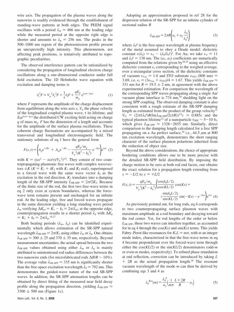
We now move on to the systematic experimental inves-tigation of short-range surface plasmon polariton resonatorsat the nanometre scale by photoemission electron micros-copy. Figure 2a shows the geometry of the microfabricatedresonator array made by electron beam lithography. Itconsists of a 6 × 6 grid, whose rod elements sample thelength interval (50-925 nm) in steps of 25 nm. The SEMimage of one particular nanorod is visible in Figure 2b. Thesesubwavelength objects were illuminated by the infrared lightof a pulsed femtosecond laser.
Panels c and d of Figure 2 report the experimental PEEMimages of the 6 × 6 resonator grid acquired at specificexcitation wavelength. The PEEM pictures correspond towide fields of view so as to embrace the whole 6 × 6resonator matrix and correspond to normal (c) or grazing(d) incidence. Experimentally, a full set of PEEM pictureshas been recorded at different wavelengths covering the range(740-880 nm).
For comparison, panels e and f of Figure 2 shows thecomputed spectral response of the rod resonator grid undernormal and grazing incidence, respectively. For each rodlength L, the displayed number is the calculated resonancewavelength λ0
Res(m) with R ) 16.5 nm; the spot area isproportional to the resonance intensity and its color indicatesthe m-resonance order. Experimentally the near field profile,i.e., the charge distribution along the rod longitudinal axis,is proportional to ∂xF. In the current PEEM experiment, theelectron emission has its origin in a three-photon absorption
process, so the resonance intensity is taken as ∫-L/2+L/2(∂xF)6
dx. According to the developed model, even and odd m orderresonances can be discriminated by an appropriate choiceof the incidence angle. Indeed, under normal incidence (k|) 0), resonances of even m order (resonances of the secondterm in eq 4) are systematically extinguished. Optically, evenorder resonances correspond to symmetric distributions ofspatially stationary surface charges and are thus forbidden.
Considering the simplicity of the resonator model used(homogeneous surrounding media, cylindrical rods, no fittingparameters), the agreement between theory and experimentis remarkable. Indeed, the main experimental spectral featuresare covered by the model. For resonator lengths in the range(50-175 nm) (top line), only three objects (100, 125, 150)nm exhibit strong resonances in the probed wavelengthwindows. As shown in the next paragraph, high-resolutionPEEM images prove that these resonances correspond to theexpected lowest-order dipolar mode m ) 1. The second (200nm e L e 325 nm) and third (350 nm e L e 475 nm) linesare of particular interest. Experimentally the second line isextinguished under normal incidence but exhibit strongPEEM signal under grazing ones in agreement with system-atic extinction of m ) 2n mode under normal incidence. Theexact opposite is observed for the third line; while excitationunder normal incidence leads to significant electron emission,no signal is detected at grazing illumination in agreementwith numerical estimates. As expected, the longer the rodlengths, the higher the resonance orders. For example,
Figure 2. Systematic Au nanorod array investigation. (a) Geometry of the microfabricated sample. The L (nm) rods are organized accordingto a 6 × 6 matrix grid, 80 µm in side. Objects are 10 µm apart. The rod length samples the interval (50-925 nm) in steps of 25 nm. (b)SEM picture of the L ) 375 nm Au nanorod. Scale bar is 100 nm. (c) PEEM imaging of the 6 × 6 resonator grid under IR laser lightillumination. Field of view 80 µm, incidence angle R ) 0°, excitation wavelength λ0 ) 790 nm, incident power P ) 40 MW/cm2, longitudinalexcitation field. Color scale is logarithmic. (d) Same as (c) but with incidence angle R ) 75°, λ0 ) 802 nm, P ) 70 MW/cm2, p polarization.Note that the PEEM signal-to-noise ratio is increased in (d) compared to (c). (e, f) Computed spectral responses of the SR-SPP resonatorgrid. For each rod length L, the displayed number is the predicted resonance wavelength λ0
Res (m), the spot area is proportional to theresonance intensity with LSR-SPP ) 3300 nm and taking into account a three-photon absorption process (logarithmic scale), the spot colorindicates the m-resonance order. Rod radius is R ) 16.5 nm. (e) Normal incidence R ) 0°. (f) Grazing incidence R ) 75°.
938 Nano Lett., Vol. 8, No. 3, 2008
resonators of length L ) 650–775 nm (Figure 2f bottom line– 1) show resonances corresponding to m ) 5.
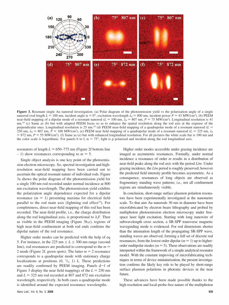
Single object analysis is one key point of the photoemis-sion electron microscopy. So, spectral investigation and high-resolution near-field mapping have been carried out toascertain the optical resonant nature of individual rods. Figure3a shows the polar diagram of the photoemission yield fora single 100 nm rod recorded under normal incidence at 800nm excitation wavelength. The photoemission yield exhibitsthe polarization angle dependence expected for a dipolarresonance (m ) 1) presenting maxima for electrical fieldparallel to the rod main axis (lightning rod effect33). Forcompleteness, direct near-field mapping of this rod has beenrecorded. The near-field profile, i.e., the charge distributionalong the rod longitudinal axis, is proportional to ∂xF. Thenas visible in the PEEM imaging (Figure 3b,c), regions ofhigh near-field confinement at both rod ends confirms thedipolar nature of the rod resonance.
Higher order modes can be predicted with the help of eq5. For instance, in the 225 nm e L e 300 nm range (secondline), rod resonances are predicted to correspond to the m )2 mode (Figure 2f, green spots). The latter m ) 2 resonancecorresponds to a quadrupolar mode with stationary chargelocalizations at positions (0, 1/2, 1) L. These predictionsare readily confirmed by PEEM imaging. Panels d-f ofFigure 3 display the near field mappings of the L ) 250 nmand L ) 325 nm rod recorded at 807 and 872 nm excitationwavelength, respectively. In both cases a quadrupolar modeis identified around the expected resonance wavelengths.
Higher order modes accessible under grazing incidence areimaged as asymmetric resonances. Formally, under normalincidence a resonance of order m results in a distribution ofnear-field peaks along the rod axis with the period L/m. Undergrazing incidence, the L/m period is roughly preserved; howeverthe predicted field intensity profile becomes asymmetric. As aconsequence, resonances of long objects are observed asfragmentary standing wave patterns; i.e., not all confinementregions are simultaneously visible.
In conclusion, short-range surface plasmon polariton resona-tors have been experimentally investigated at the nanometrescale. To that aim Au nanorods 30 nm in diameter have beenmicrofabricated by electron beam lithography and probed bymultiphoton photoemission electron microscopy under free-space laser light excitation. Starting with long nanowire ofsubwavelength cross section, a SR-SPP transverse magneticwaveguiding mode is evidenced. For rod dimensions shorterthan the attenuation length of the propagating SR-SPP wave,standing waves are observed, forming a full set of discrete rodresonances, from the lowest order dipolar (m ) 1) up to higher-order multipolar modes (m ) 5). These observations are readilyinterpreted within the framework of a simple analytical resonatormodel. With the constant improving of microfabricating tech-niques in terms of device miniaturization, the present investiga-tion confirms the likely key role to be played by short-rangesurface plasmon polaritons in photonic devices in the nearfuture.
These advances have been made possible thanks to thehigh resolution and local-probe-free nature of the multiphoton
Figure 3. Resonant single Au nanorod investigation. (a) Polar diagram of the photoemission yield vs the polarization angle of a singlenanorod (rod length L ) 100 nm, incident angle R ) 0°, excitation wavelength λ0 ) 800 nm, incident power P ) 43 MW/cm2). (b) PEEMnear-field mapping of a dipolar mode of a resonant nanorod (L ) 100 nm, λ0 ) 807 nm, P ) 75 MW/cm2). Longitudinal resolution is 41nm.19 (c) Same as (b) but with adapted PEEM focus so as to enhance the spatial resolution along the rod axis at the expense of theperpendicular ones. Longitudinal resolution is 25 nm.19 (d) PEEM near-field mapping of a quadrupolar mode of a resonant nanorod (L )250 nm, λ0 ) 807 nm, P ) 100 MW/cm2), (e) PEEM near field mapping of a quadrupolar mode of a resonant nanorod (L ) 325 nm, λ0
) 872 nm, P ) 55 MW/cm2). (f) Same as (e) but with enhanced longitudinal resolution. For all pictures the white scale bar is 100 nm andthe color scale is logarithmic. For panels b to f, R ) 75°, light is p polarized and incident along the rod longitudinal axis.
Nano Lett., Vol. 8, No. 3, 2008 939
PEEM technique. Further improvements will take care ofthe presence of an interface and the exact geometry of thenanorod cross section.
Acknowledgment. The authors from CEA Saclay thankF. Merlet for expert technical support during PEEM experi-ment and A. Ghorbal for additional atomic force microscopystudies.
References(1) Barnes, W. L.; Dereux, A.; Ebbesen, T. W. Nature 2003, 424, 824–
830.(2) Greffet, J. J. Science 2005, 308, 1561–1562.(3) van Hulst, N. F. Nature 2007, 448, 141–142.(4) Taminiau, T. H.; Moerland, R. J.; Segerink, F. B.; Kuipers, L.; van
Hulst, N. F. Nano Lett. 2007, 7, 28–33.(5) Stockman, M. I. Phys. ReV. Lett. 2004, 93, 137404–137407.(6) Søndergaard, T.; Bozhevolnyi, S. Phys. ReV. B 2007, 75, 73402–73405.(7) Muhlschlegel, P.; Eisler, H. J.; Martin, O. J. F.; Hecht, B.; Pohl, D. W.
Science 2005, 308, 1607–1609.(8) Cubukcu, E.; Kort, E. A.; Crozier, K. B.; Capasso, F. Appl. Phys.
Lett. 2006, 89, 93120–93122.(9) Neubrech, F.; Kolb, T.; Lovrincic, R.; Fahsold, G.; Pucci, A.; Aizpurua,
J.; Cornelius, T. W.; Toimil-Molares, M. E.; Neumann, R.; Karim, S.Appl. Phys. Lett. 2006, 89, 253104–253106.
(10) Payne, E. K.; Shuford, K. L.; Park, S.; Schatz, G. C.; Mirkin, C. A.Journal of Physical Chemistry B 2006, 110, 2150–2154.
(11) Cinchetti, M.; Gloskovskii, A.; Nepjiko, S. A.; Schonhense, G.;Rochholz, H.; Kreiter, M. Phys. ReV. Lett. 2005, 95, 257403–257406.
(12) Kubo, A.; Onda, K.; Petek, H.; Sun, Z. J.; Jung, Y. S.; Kim, H. K.Nano Lett. 2005, 5, 1123–1127.
(13) Munzinger, M.; Wiemann, C.; Rohmer, M.; Guo, L.; Aeschlimann,M.; Bauer, M. New J. Phys. 2005, 7, 68–83.
(14) Douillard, L.; Charra, F.; Fiorini, C.; Adam, P. M.; Bachelot, R.;Kostcheev, S.; Lerondel, G.; de la Chapelle, M. L.; Royer, P. J. Appl.Phys. 2007, 101, 83518–83522.
(15) Heringdorf, F. M. Z.; Chelaru, L. I.; Mollenbeck, S.; Thien, D.;Hoegen, M. H. V. Surf. Sci. 2007, 601, 4700–4705.
(16) Kubo, A.; Pontius, N.; Petek, H. Nano Lett. 2007, 7, 470–475.
(17) Dickson, R. M.; Lyon, L. A. J. Phys. Chem. B 2000, 104, 6095–6098.
(18) Sonnichsen, C.; Franzl, T.; Wilk, T.; von Plessen, G.; Feldmann, J.;Wilson, O.; Mulvaney, P. Phys. ReV. Lett. 2002, 88, 077402-077405.
(19) Huang, H. J.; Yu, C. P.; Chang, H. C.; Chiu, K. P.; Chen, H. M.; Liu,R. S.; Tsai, D. P. Opt. Express 2007, 15, 7132–7139.
(20) Seong Keun, K.; Okamoto, H.; Jong Kuk, L.; Imura, K.; Nagahara,T. Chem. Phys. Lett. 2005, 412, 41–45.
(21) Ditlbacher, H.; Hohenau, A.; Wagner, D.; Kreibig, U.; Rogers, M.;Hofer, F.; Aussenegg, F. R.; Krenn, J. R. Phys. ReV. Lett. 2005, 95,257403–257406.
(22) The lateral resolution is defined by the horizontal distance over whichthe intensity drops from 84% to 16% of maximum signal.
(23) The current LEEM/PEEM instrument works in total electron yieldwhich increases its sensitivity at the price of a loss of spatial resolutionoriginating from the energy spread of the electrons contributing tothe image formation (chromatic aberration).
(24) Wiederrecht, G. P. Eur. Phys. J.: Appl. Phys. 2004, 28, 3–18.(25) Nelayah, J.; Kociak, M.; Stephan, O.; de Abajo, F. J. G.; Tence, M.;
Henrard, L.; Taverna, D.; Pastoriza-Santos, I.; Liz-Marzan, L. M.;Colliex, C. Nat. Phys. 2007, 3, 348–353.
(26) Vesseur, E. J. R.; Waele, R. d.; Kuttge, M.; Polman, A. Nano Lett.2007, 7, 2843–2846.
(27) Salomon, L.; Bassou, G.; Aourag, H.; Dufour, J. P.; de Fornel, F.;Carcenac, F.; Zayats, A. V. Phys. ReV. B 2002, 65, 125409–125413.
(28) Novotny, L. Phys. ReV. Lett. 2007, 98, 266802–266805.(29) Coefficients values are computed from a1 ) 13.74 – 0.12(ε∞ +
141.04εs)/εs and a2 ) 0.12√ε∞ + 141.04εs ⁄εs. More details canbe found in ref 28.
(30) Raether, H. Springer Tracts Mod. Phys. 1988, 111.(31) Klyuchnik, A. V.; Kurganov, S. Y.; Lozovik, Y. E. Phys. Solid State
2003, 45, 1327–1331.(32) Lamprecht, B.; Schider, G.; Lechner, R. T.; Ditlbacher, H.; Krenn,
J. R.; Leitner, A.; Aussenegg, F. R. Phys. ReV. Lett. 2000, 84, 4721–4724.
(33) Van Bladel, J. G. Singular Electromagnetic Fields and Sources; WileyIEEE Press: New York, 1996; ISBN 978-0-7803-6038-9.
NL080053V
940 Nano Lett., Vol. 8, No. 3, 2008