Embed Size (px)
Citation preview
MateriaLs Science and Engineering, B5 (1990) 269- 273 269
Silicon Implantation of GaAs at Low and Medium Doses: Raman Assessment of the Dopant Activation
S. ZEKENG, B. PREVOT and C. SCHWAB
Groupe "Recherches Physiques et Matdriaux ", Centre de Recherches Nucl~;aires, University; Louis l'asteur, 23 Rue du Loess. 67037, );trasbourg Cedex (France)
(Received June 2. 19891
Abstract
Raman-scattering experiments were carried out on (001) GaAs implanted with 4 x 10 j: cm- : 100 keV or 8 x 101: cm ~: 110 keV Si + ions and then processed by conventional furnace annealing in the temperature range 400-900°C. The first-order Raman signature is found to depend strongly on both dose and annealing temperature. A careful examination of the mode intensities as a function of the annealing temperature allowed the dopant activation to be monitored. This has been con- firmed quantitatively by performing a line shape analysis of the whole first-order Raman signature.
1. Introduction
The inelastic scattering of (visible) light or Raman scattering (RS) by phonons has been widely used to characterize ion implantation damage in GaAs as well as its recovery by various thermal techniques [1-6]. On the other hand, RS by coupled phonon-plasmon modes gives access to a contactless characterization of the free- electron (hole) gas in GaAs [7]. In this process [8] the free-carrier, vibration (or plasmon) interacts with the mechanical vibration (longitudinal opti- cal (LO) phonon) giving rise to two coupled modes L and L +. The L mode appears at a frequency lower than that of the pure LO mode of the crystal, while the L + mode frequency is equal to or greater than the LO frequency, depending on the free-carrier concentration. This picture is valid in the limit of vanishing scattering wave- vector (q=0) [9] or for a negligible damping factor of the carriers (high mobility regime) [5]. Most of the previous studies report on the dis- persion relation of the coupled modes or on the wavevector-dependent dielectric response of the electron gas [10[. They have been carried out on
high quality melt-grown doped materials or epitaxial layers.
In GaAs samples implanted with n-type dopants the situation is slightly different. The process of doping is more difficult in these sam- ples since it necessitates a subsequent treatment to remove the associated lattice damage and electrically activate the implanted atoms. On the other hand, the signal analysis might be further complicated by both the actual distribution of the carriers and the presence of a surface-depleted layer as observed in III-V doped semiconductors [11].
The purpose of this paper is to show that RS is also a convenient method for the assessment of the dopant activation in silicon-implanted GaAs substrates even for rather low doses, e.g. 4 × 10¹² ions cm -2, which are typical in metal-Schottky field effect transistor (MESFET) technology. We found that the first-order RS signature is strongly dependent on both the initial dose and the annealing temperature 7,~. From a detailed analysis of the spectra we were able to describe the activation behaviour in the low and medium implantation cases. Further, in certain conditions, a line shape analysis based on a simple two-layer model was shown to give quantitative results for the active region.
2. Experimental details
Liquid-encapsulated Czochralski grown chromium-doped semi-insulating GaAs (001)- oriented substrates, capped with a reactively sputtered Si3N 4 layer 50 nm thick, have been implanted at room temperature with Si + ions with a fluence of 4 x 1012 cm 2 (100 keV) or 8 x 10 ~3 cm -2 (110 keV). The thermal treatment consisted of separate annealings (12 rain) per-
0921-5107/90/$3.50 © Elsevier Sequoia/Printed in The Netherlands
270
formed in flowing argon gas between 400 and 900 °C in steps of 50 °C. All RS experiments were performed at room temperature using the 488 nm line ( h % = 2.54 eV) of an Ar + ion laser and without removing the protective cap. It was observed, however, that at the highest tempera- ture the sputtered Si3N 4 layer sometimes bubbled and/or lost adhesion. This resulted in a poor signal-to-noise ratio for the corresponding spectra. Most of the spectra were measured in the Brewster angle configuration (i B = 77 °) from the (001) surface with the incident light polarized along a [110] crystallographic direction. In some cases the true backscattering geometry ( i=0 °) was also used. In both instances the scattered light, unanalysed for its polarization, was col- lected normal to the sample surface and analysed with a double monochromator equipped with a cooled Quantacon photomultiplier working in the photon-counting mode. The instrumental resolu- tion was set at 3 cm- ~.
In the true backscattering geometry from a (001) surface of a sphalerite symmetry crystal, it is well known that only the LO mode is observ- able in the first-order RS spectrum [8]. If the Brewster angle configuration is used, the wave- vector of the incident light makes an angle of 13 ° with the [001] crystal axis, thus leading to a weak participation of the transverse optical (TO) mode in the spectrum. From an exact calculation, the ratio R0(T/L ) of the transverse over the longi- tudinal intensities is predicted to be 0.12 in a perfect and undoped GaAs specimen [12]. Any significant deviation from this value will be inter- preted in terms of either a loss of perfection in the crystalline structure of the sample or the presence of free carriers in the investigated layer.
3. Results
Whatever the dose, the spectra recorded after implantation consist of two contributions: the first-order LO and TO peaks at q = 0, but slightly modified (red shifted), and three broad and more or less intense bands which originate from amor- phized regions. These structures are known to mirror the broadened one-phonon density of states of the corresponding crystal, permitted by the relaxation of the momentum conservation rule [3, 5, 6].
Figure 1 shows a series of RS spectra of GaAs implanted at low dose (4×1012 cm -2) and annealed at temperatures ranging from 500 to
~, iO'z r m 3 :0 ~ ',
• _ '77 ~'. ' - z < ~ e ,
<2.'3} 50@%
z
z
_ 7 0 ~ 0 ° r
BO0°(
~00°(
r,~
2hO 30% '-
F i g . 1. First-order Raman spectra of Si +-implanted (4 x 10 ~ cm -~, 100 keV) GaAs annealed at the temperatures indi- cated. The spectra have been obtained in the Brewster angle configuration (i. = 77°). Vertical arrows refer to Ar + plasma lines used for energy calibration purposes. (The same is valid for Figs. 2 and 3.)
900 °C. In this figure, all spectra have been drawn on the same ordinate scale, with the exception of the upper one. After the T~ = 500 °C annealing, the first-order RS signal looks almost perfect with respect to either the peak position of the modes or their intensity ratio. For annealings performed at higher temperatures, the spectra suffer marked modifications with respect to the LO line only. This line is first reduced in magnitude while pronounced wings are observed around its basis for T.~= 800 °C (and also for 850 °C) and then it seems to recover its former characteristics. In contrast, the TO line does not show any line shape or intensity variation.
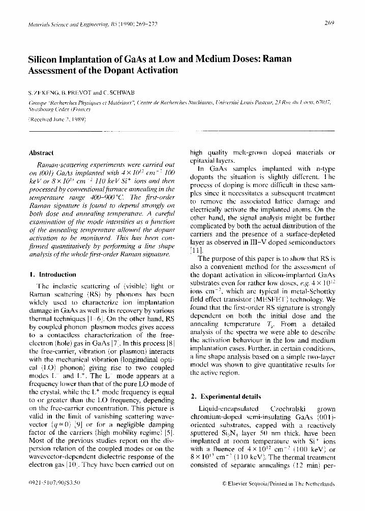
For the medium-dose-implanted sample (8x 1013 cm -2) we observe quite a different behaviour, as depicted in Fig. 2. Starting from a spectrum almost typical of an unimplanted sample (T.~ = 650 °C), a modification of the LO part of the spectrum is first observed for T. d = 700 °C and then a progressive alteration of the TO part for T a > 750 °C, the LO mode inten-
! Si • . (SisNJGQAs} J [ ( 8×1013cm -~ 110 keV) : i B : ? 7 o hv t : 2 . 5L , eV
i ji
r[, " ,SO0°C /
,0 i l l
, ~ 750°C
< @ - - ~ ~ [ z - . . . . ! . .... .4~. "~
- a ~ H
!i: I ,
.... To Lo ................ ] ...... !
240 210 320 360 STOKES SHIFT(cm -1)
Fig. 2. F i r s t -o rde r Raman spect ra of Si +-implanted (8 x 1013 cm e 110 keV) G a A s annealed at different tempera tures . T h e traces have been d rawn with different magnif icat ion rates as indicated.
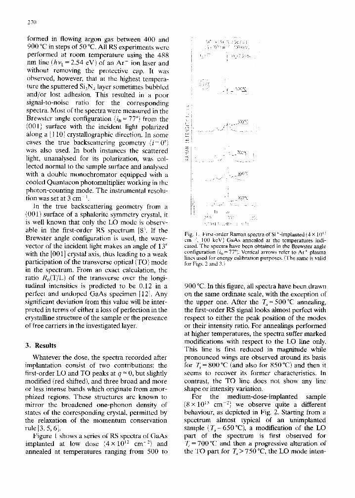
sity continuing however to decrease until the ultimate T.~. In order to clarify the origin of such a modification observed around the TO frequency, RS spectra were measured on the same samples but in true backscattering configuration, in which theory predicts that the TO mode cannot be observed in a non-resonance situation. A selected series of these spectra are shown in Fig. 3, from which it becomes obvious that a new signal is growing up at a frequency nearly equal to that of the TO mode. It is believed that it arises from the coupling effect between the purely mechanical vibrations (LO phonon) and the electronic ones (plasmon), thus explaining the observations previ- ously reported in Fig. 2. In spite of experimental investigations performed at higher energy trans- fer (up to 800 cm -1) in order to find an L + coupled mode, no significant signal was observed in these samples. It follows that in the present cases any direct determination of the free-carrier concentration cannot be performed from only the frequency of the L + coupled mode.
Si + ~ ( Sis No./Go As ) (8×101?cm -2 - 110keY)
i : 0 ° II hVL: 2" 5/+eV
271
i! - , All o_ I
- - , £- I 0 j ; 3,- ~ - - - - ~ "
j Z LJ l - -
i
Z <
650°E J
, . . ~ , %0°E ii :× 25) : - -
l
I
850°(
2@
L 0 •
L _ I ~ i 280 320 360
STOKES SHIFT(era -I)
Fig. 3. F i r s t -o rder Raman spect ra of Si +- implanted (8 x 1013 cm -, 110 keV) G a A s recorded in the backscat tef ing geomet ry (i = 0 °) for different anneal ing steps.
4. Analysis and discussion The proposed analysis is based on the com-
parison of the different depths which are relevant to the present study, i.e. the thicknesss of the implanted layers, the optical penetration depth of the laser light and possibly the depth of the free- carrier-depleted zone. The optical penetration depth Xop t depends on the absorption coefficient: at hVL= 2.54 eV we get Xop ~ = 80 nm for GaAs [13] (1/e attenuation), taking into account that Si3N 4 is transparent at that photon energy. The width of the implanted layer may be approxi- mated by the projected range Rp, which depends on the impinging ion nature and energy and the target material properties. In the actual conditions we obtain Rp of about 50 and 60 nm respectively for the low and medium fluences. In the Schottky barrier formalism the depleted zone X d is known to vary as the inverse function of N ~/e, where N is the carrier concentration. In the present case X d decreases from about 100 nm (N=I ×1017 cm 3) to 25 nm (N=2× 10 Is cm-3). It is thus justified to state the following conditions:
272
Xd ~ Rp ~ Xopt (1)
We then suppose that in the optical depth Xop t the Raman signal with longitudinal symmetry arises from two layers involving different scattering mechanisms. From the depleted zone a pure unscreened LO signal is expected, while in the activated region underneath (width Xop t - X i ) a coupled LO phonon-plasmon contribution is assumed. The TO mode, being unaffected by the electron gas, instead originates from the whole Xop , depth. From the above considerations we obtain
R(T/L)°CRo(T /L)Xop t /X d with Xd ~< Xom (2)
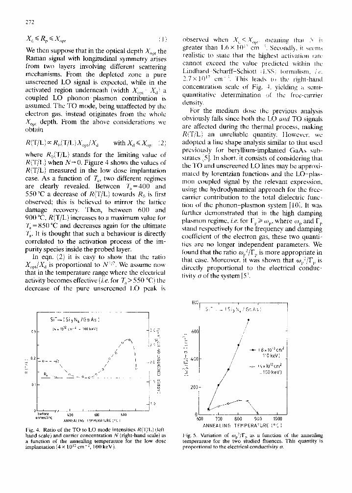
where R0(T/L ) stands for the limiting value of R(T/L) when N--* 0. Figure 4 shows the values of R(T/L) measured in the low dose implantation case. As a function of Z~, two different regimes are clearly revealed. Between 77~=400 and 550 °C a decrease of R(T/L) towards R0 is first observed; this is believed to mirror the lattice damage recovery. Then, between 600 and 900 °C, R(T/L) increases to a maximum value for 7~, = 850 °C and decreases again for the ultimate 7;. It is thought that such a behaviour is directly correlated to the activation process of the im- purity species inside the probed layer.
In eqn. (2) it is easy to show that the ratio Xopt/X d is proportional to N 1/2. We assume now that in the temperature range where the electrical activity becomes effective (i.e. for 71, > 5 50 °C) the decrease of the pure unscreened LO peak is
0.3
_ 0.2
Ix
Si + - ( S i 3 N ~ . / G o A S )
{(" x 1012 cm -2 - 100 keV}
o f ° \ i % ~25 /
- o - - -41 f t ~20 \ / I l
R 0 O ~ ~
°--°I" ~1 5
Ol r <
0 I // I I I I I I 1 1 0
before &O0 600 800 onneol ing
ANNEALING TEMPERATURE { °C)
Fig. 4. Ratio of the TO to LO mode intensities R(T/L) (left- hand scale) and carrier concentrat ion N (right-hand scale) as a function of the annealing temperature for the low dose implantation (4 x 1012 cm 2, 100 keV).
observed when X a <:A~op~. meaning that 'v is. greater than 1.6 x 10 ~7 cm , Secondly, it seems realistic to state that the highest activation ral~- cannot exceed the value p~edicted within the Lindhard-Scharff-Schiotl <I,SSI formalism, i.u. 2 .7x10 ~ cm ~. This leads t~ lhe right-hand concentration scale of Fig. 4, yielding a semi- quantitative determination of the free-carrier density.
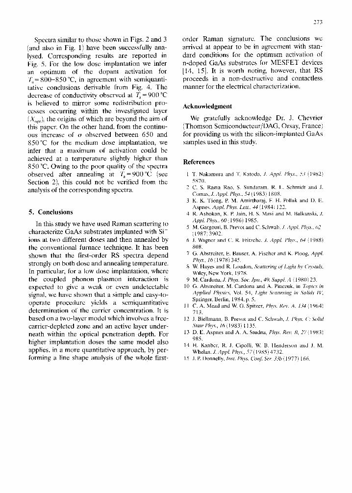
For the medium dose the previous analysis obviously fails since both the LO and TO signals are affected during the thermal process, making R(T/L) an unreliable quantity. However, we adopted a line shape analysis similar to that used previously for beryllium-implanted GaAs sub- strates [5]. In short, it consists of considering that the TO and unscreened LO lines may be approxi- mated by lorentzian functions and the LO-plas- mon coupled signal by the relevant expression, using the hydrodynamical approach for the free- carrier contribution to the total dielectric func- tion of the phonon-plasmon system [10]. It was further demonstrated that in the high damping plasmon regime, i.e. for Fp > (%, where %, and Fp stand respectively for the frequency and damping coefficient of the electron gas, these two quanti- ties are no longer independent parameters. We found that the ratio a)p2/F e is more appropriate in that case. Moreover, it was shown t h a t O)p2/Fp is directly proportional to the electrical conduc- tivity o of the system [5t.
600 "i E u
~00 N a -
3
800 , ,
F Si* - (S i3N ~ G o A s )
1' f
/ /
_,__ ( 8 x1013cm 2 ! I0 keV) /
.... (4xlOUcrn 2 _100 keV)
20@
o I I
600 700 800 900 1000
ANNEALIN6 TEMPERATURE (of)
Fig. 5. Variation of a * 2/Fp as a function of the annealing P
temperature for the two studmd fluences. This quantity is proportional to the electrical conductivity o.
273
Spectra similar to those shown in Figs. 2 and 3 (and also in Fig. 1) have been successfully ana- lysed. Corresponding results are reported in Fig. 5. For the low dose implantation we infer an optimum of the dopant activation for T.~= 800-850 °C, in agreement with semiquanti- tative conclusions derivable from Fig. 4. The decrease of conductivity observed at T~, = 900 °C is believed to mirror some redistribution pro- cesses occurring within the investigated layer (X,,pt), the origins of which are beyond the aim of this paper. On the other hand, from the continu- ous increase of o observed between 650 and 850°C for the medium dose implantation, we infer that a maximum of activation could be achieved at a temperature slightly higher than 850 °C. Owing to the poor quality of the spectra observed after annealing at Z ,=900°C (see Section 2), this could not be verified from the analysis of the corresponding spectra.
5. Conclusions
In this study we have used Raman scattering to characterize GaAs substrates implanted with Si + ions at two different doses and then annealed by the conventional furnace technique. It has been shown that the first-order RS spectra depend strongly on both dose and annealing temperature. In particular, for a low dose implantation, where the coupled phonon-plasmon interaction is expected to give a weak or even undetectable signal, we have shown that a simple and easy-to- operate procedure yields a semiquantitative determination of the carrier concentration. It is based on a two-layer model which involves a free- carrier-depleted zone and an active layer under- neath within the optical penetration depth. For higher implantation doses the same model also applies, in a more quantitative approach, by per- forming a line shape analysis of the whole first-
order Raman signature. The conclusions we arrived at appear to be in agreement with stan- dard conditions for the optimum activation of n-doped GaAs substrates for MESFET devices [14, 15]. It is worth noting, however, that RS proceeds in a non-destructive and contactless manner for the electrical characterization.
Acknowledgment
We gratefully acknowledge Dr. J. Chevrier (Thomson Semiconducteur/DAG, Orsay, France) for providing us with the silicon-implanted GaAs samples used in this study.
References
1 T. Nakamura and T. Katoda, J. Appl. Phys'., 53 (1982) 587(I.
2 C. S. Rama Rao, S. Sundaram, R. E. Schmidt and J. Comas, J. Appl. Phys., 54 (1983) 18(/8.
3 K. K. Tiong, R M. Amirtharaj, E H. Pollak and D. E. Aspnes, Appl. Phys. Lett., 44 (1984) 122.
4 R. Ashokan, K. P. Jain, H. S. Mavi and M. Balkanski, J. Appl. Phys., 60(1986) 1985.
5 M. Gargouri, B. Prevot and C. Schwab, J. Appl. Phys., 62 (1987) 3902.
6 J. Wagner and C. R. Fritzche, J. Appl. Phys., 04 (1988) 808.
7 G. Abstreiter, E. Bauser, A. Fischer and K. Ploog, Appl. Phys., 16 (1978) 345.
8 W. Hayes and R. Loudom Scattering of Light by Crystals. Wiley, New York, 1978.
9 M. Cardona, J. Phys. Soc. Jpn., 49, Suppl. A (1980) 23. 10 G. Abstreiter, M. Cardona and A. Pinczuk, in Topics in
Applied Physics, Vol. 54, Light Scattering in Solids IV, Springer, Berlin, 1984, p. 5.
11 C.A. Mead and W. G. Spitzer, Phys. Rev. A, 134 (1964) 713.
12 J. Biellmann, B. Prevot and C. Schwab, J. Phys. (': Solid State Phys., 16 (1983) 1135.
13 D. E. Aspnes and A. A. Studna, Phys. Rev. B, 27(1983) 985.
14 H. Kanber, R. J. Cipolli, W. B. Henderson and J. M. Whelan, J. Appl. Phys., 57 (1985) 4732.
15 J.P. Donnelly, lnst. Phys. Conf. Ser. 33b (1977) 166.


![1001 J - diagramasde.comdiagramasde.com/diagramas/otros/1001 Circuitos [Parte10].pdf1001 •ELEKTOR• circuits Comme, en principe, le MGA-72543 est composé d’un étage à FET GaAs,](https://img.pdfslide.fr/doc/110x75/5b0ab1427f8b9adc138c85f6/1001-j-circuitos-parte10pdf1001-elektor-circuits-comme-en-principe.jpg)