Embed Size (px)
Citation preview
ELSEVIER Surface Science 334 (1995) 329-341
~.~i ~ ' ~ * : ~ ................................... ~:~:it~'~.-~i ~
surface science
..... ~ # i ~ i ~ i ~ ~'."
Theoretical study of the secondary electron emission of insulating targets
J.P. Ganachaud *, A. Mokrani Groupe de Physique des Mat&iaux pour l'Electronique, EA 1153, Laboratoire de Physique du Solide Th£orique, Facult~ des Sciences et
des Techniques, Universit~ de Nantes, 2 Rue de la Houssiniere, 44072 Nantes Cedex 03, France
Received 2 January 1995; accepted for publication 21 March 1995
Abstract
We study the electron-induced secondary electron emission of insulating targets by a Monte-Carlo simulation method. The most important collision mechanisms in the energy domain considered are investigated. The usual approximations apparently overestimate the elastic collision rate and empirical corrections are proposed. The self-trapping of the charges is explained by the polarization of the surrounding medium. The role of the polaronic effects in the Secondary emission as well as the sensibility of the results to the choice of the different parameters are analyzed. The influence of an internal electric field caused by a "frozen" charge distribution is also investigated.
Keywords: Aluminum oxide; Computer simulations; Dielectric phenomena; Electron-solid interactions; Field effect; Insulating films; Secondary electron emission
1. Introduction
For a realistic description of the secondary elec- tron emission of insulating targets, one needs to know how an electron interacts with the various components of the sample. The corresponding en- ergy domain practically ranges from the primary beam energy down to a fraction of an eV and the interaction cross-sections can vary rapidly with the energy of the electron.
When its energy E (reckoned from the bottom of the conduction band) exceeds the energy gap (E > Eg = 10 eV), an electron can produce individual electron transitions from the valence band to the conduction one. It can also suffer elastic collisions
* Corresponding author.
by interacting With the potentials which Surround the various ions of the solid. When its energy is suffi- cient, it can also interact inelastically with the elec- trons of the inner-shells of the ions and cause their ionization:
At lower electron energies (E < Eg), the inelastic effects are mainly due to the electron-phonon colli- sions. The electron can always interact with:~the potentials surrounding the ions but a Static potential model may turn to be inadequate and a conventional approach may strongly overestimate the importance of the elastic effect.
When its energy becomes sufficiently i0w, /an electron, by locally distorting the ltittice, can~consid- erably reduce its mobility. This " p o l a r o n i c , effect, assisted by the presence of defects or o f other inho- mogeneities in the sample can give rise to-charge trapping.
0039-6028/95/$09.50 © 1995 Elsevier Science B.V. All rights reserved SSDI 0 0 3 9 - 6 0 2 8 ( 9 5 ) 0 0 4 7 4 - 2
330 J.P. Ganachaud, A. Mokrani / Surface Science 334 (1995) 329-341
In an insulator bombarded by an electron beam, regions of positive and negative charging-up appear. For the energy domain considered in the present study, the density of charge is always positive near the surface and becomes negative in the bulk of the solid. Analytical expressions have been proposed to represent this charge and the electrical field which results from it.
In Section 2 of this paper we present our model for the interaction of an electron with an insulating target and we determine the cross-sections for the different collisions. The model is not able to account for specific effects due to the crystalline nature of the sample. Thus it can be considered as mainly adapted for amorphous targets or for polycrystals. The values of the parameters used to carry out the present calculations have been obtained from the data available in the literature for amorphous alu- mina.
In this section, some corrections for the elastic cross-sections at low energies are proposed and the concept of charge trapping via the polaronic effect is also analyzed.
In Section 3 we present our results. We discuss in detail the influence of different parameters of the model and we introduce the effect of the electrical field.
The conclusions are presented in Section 4.
2. Electron-insulator interaction model
2.1. Electron-electron collisions
An electron with an energy higher than the band gap can excite electron-hole pairs. The electron which is promoted from the valence band to the conduction one can then take part in the transport process. We shall presently assume, for the sake of simplification, that in the relaxation of the valence band hole the energy is transferred to the band as a whole so that this process does not significantly contribute to the emission of secondary electrons.
The energy loss AE and the momentum transfer hq suffered by an electron in a collision within a delocalized electron gas can be expressed from the dielectric theory by considering the loss function I m ( - 1 / ~ ( q , A E ) ) , where ~(q,AE) is the dielectric
function for the medium. The differential probability of a collision per unit path length is
% ~ ( E ; A E , q ) - - - Im . (1) ~-a 0 E q e ( q , A E )
In a free electron material, within the random phase approximation, E(q, AE) can be conveniently assimilated to the Lindhard function [1]. We can then distinguish in %1 contributions due to the excitation of electron-hole pairs from collective ones corre- sponding to plasmon creation. However, in the case of an insulator, the above approximations loose much of their significance. A possible approach is to re- place simply E(q,AE) by e(0,AE) [2,3] and also sometimes to replace in practice E(0,AE) by its optical equivalent E(h w) where h w --- AE.
In an ionic solid, an electron interacts with a charge distribution which presents strong spatial in- homogeneities. So it seems important to account for a local field which can differ markedly from the mean field which corresponds to the q = 0 limit.
Several authors, such as Tung et al. [4], Penn [5], and Tanuma et al. [6], have developed some methods for extending the determination of E(0,AE) to non- zero values of q.
We have also previously proposed [7,8] an empir- ical method to introduce the local field effects by using the following expression, where Im(-1/E(q, AE)) is approximated by a separable function of q and AE:
%1( E;AE,q) -- - - O~q Im • "a0 E q e ( A E ) "
(2) In the expression Olq --- (1 + bqq) "1 and bq is the
"local field" parameter. The probability of an electron-electron collision
per unit path length is then given by
O'~l( E) = fE~ d( AE) fqql~l( E;AE,q) d q, (3)
where ql and q2 represent the limits for the momen- turn transfer that an electron can undergo in a colli- sion in the free electron scheme.
Swanson [9] has measured the dielectric function of polycrystalline "y-A1203 films as well as that of amorphous A1203 anodized films, from characteris- tic energy loss experiments. In our calculations, we
J.P. Ganachaua~ A. Mokrani / Surface Science 334 (1995) 329-341 331
have used the values for amorphous alumina given in Ref. [9]. These latter agree well with the results obtained from optical measurements by Arakawa and Williams [10] with the same type of targets.
In Ref. [9], the energy losses A E range from 6 to 35 eV. They present a marked maximum near 25 eV, which manifests itself as a broad peak that can be attributed to a bulk plasmon excitation. We have extended these values beyond 35 eV by assuming a simple law in A / A E " . With A = 1.6 X 10⁵ and n = 3.75, a reasonable agreement with the sum rules [11] is obtained at high energies.
In the present model, it is admitted that the major process for bulk plasmon damping is a local one and that it essentially gives rise to the creation of one electron-hole pair. So, the collective excitation, which strongly contributes to the experimental loss function, has not practically to be distinguished from the individual excitations with regard to the sec- ondary electron emission. The experimental energy loss spectrum presents some features that can be attributed to surface excitations but, in practice, they have not been distinguished from the bulk excita- tions in our calculations.
A value for the local field parameter bq used in relation (2) can be estimated by trying to reproduce as well as possible the variation with the energy of a reference mean free path such as that proposed by Tanuma et al. [12]. This latter seems to account correctly for the known experimental values, for a large variety of samples, and is in rather good agree- ment with the relation proposed by Seah and Dench [131.
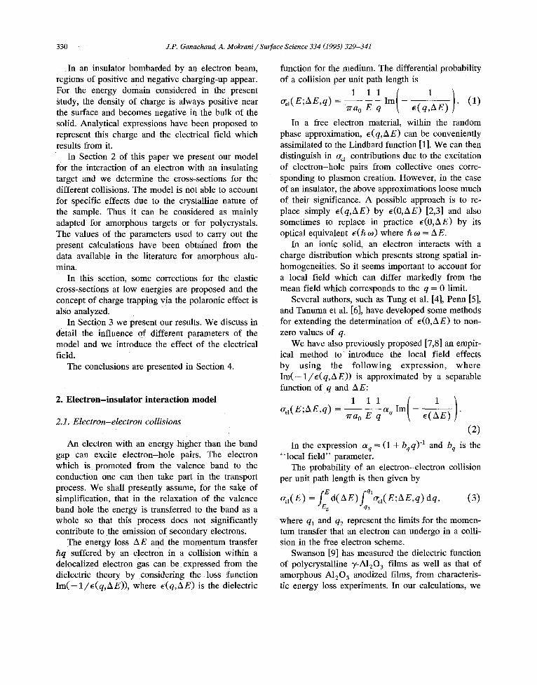
If we write the local field parameter under the form bq = aq/(E1R/aao), where E R is the Rydberg energy and a 0 the Bohr unit, a value of the local field parameter corresponding to aq = 0.1 seems to reproduce nearly perfectly the variations of A given by Tanuma et al., in all the energy domain ranging from 50 to 1500 eV, as can be seen in Fig. 1.
The energy of an electron excited out of the valence band, either by the direct creation of a pair or by plasmon damping, is determined by the non-di- rect transition model [2,7,14]. The probability for the energy AE to be transferred to an initial energy level E 0 of the valence band is assumed to be proportional to the product of the densities of states:
P ( Eo,A E ) = Cn( Eo)n ( E o + AE) , (4)
12
K Ii • . J
e -
"-" 6
', 'i, i "q = i o-=_L.--:--(
. . . . . . . i . . . . . . . L . . . . . . i. o.o
= i i . . . . . . . . . . . . . . . . . . . . . . . . . . . . . . . . . . . . . . . . . . . . . . . . . . . .
0 i I _ 0 20 40 60 80 100
E (eV)
Fig. 1. Inelastic electron-electron collision mean free path calcu- lated from the dielectric theory for different values of the local field parameter aq. The crosses correspond to the calculations of Tanuma et al. [12].
where C is a constant and n is the density of states. This latter is assumed to vary like ~ for the conduction band. The valence band is made of two sub-bands which are rectangular in shape, one lying from - 9 to - 16.3 eV, with 6 electrons per molecule of A1203, and the other lying from - 24.8 to - 28.1 eV and containing 2 electrons [15].
From classical arguments we assume that, after the collision, the excited electron moves in a direc- tion perpendicular to that of the other particle and that its momentum vector lies in the incidence plane, defined by the directions of the incident particle before and after collision.
2.2. Inner-shell ionizations
The classical formalism of Gryzinski [16] has been retained to describe the inelastic interactions of an electron with the inner shells of the ions. In alumina, for primary energies Ep < 1.5 keV, only three atomic levels have to be considered: AI2p, Al2s and O ls, for which the ionization potentials are 77, 124 and 533 eV, respectively [17]. In prac- tice, only the two first levels contribute significantly at these primary energies. For A1203, there are approx ima te ly Nat = 100 atoms per nm 3, that is 40 aluminum atoms and 60 oxygen atoms per nm 3.
Even if the mean free paths for these collisions are very large, of the order of one hundred times the
332 J.P. Ganachaud, A. Mokrani / Surface Science 334 (1995) 329-341
electron-valence band one, their stopping power re- mains appreciable and their contribution to the sec- ondary electron emission is non-negligible.
Concerning the angular aspect of these collisions, from classical arguments, the deflection angle O suffered by the incident electron can be calculated by the relation
sin20 = AE/E, (5)
where AE is the energy transferred to an inner-shell electron. It is assumed that this particle is ejected in a direction perpendicular to the direction followed by the ionizing electron after the collision.
The relaxation mechanisms which follow the ion- ization of an inner-shell (radiative transitions or Auger effects involving the deep hole) have not been taken into account in our calculations.
2.3. Electron-phonon collisions
At low energies, when E does not exceed two or three times the value of the gap Eg, an electron has an important probability to interact with the lattice vibrations.
The interaction of a quasi-free electron with the longitudinal optical (LO) phonons in a polar medium can be treated by FrShliCh's perturbation theory [18] (see for instance Llacer and Garwin [19] or Fitting and Friedmann [20]).
The interaction with the lattice is accompanied by the creation or by the absorption of a phonon. For the optical branch, it is reasonable to ignore the dispersion relation of the longitudinal phonon and to characterize it by the unique frequency O)LO.
An electron with the energy E has a probability per unit of path length to create a phonon of fre- quency w and so to lose the energy AE = hto given by (,+1)(1 1)1
- 5 - - i(o) a0 [I1+ :,11 I Xln [ 1 / 2 ] ,
AE
E
(6)
where nq represents the occupation function for the phonon level at temperature T, taken here equal to 300 K. e(0) represents the static dielectric constant and E(~) is the high frequency or optical one.
A similar expression can be obtained for the phonon absorption rate o-p~(E).
Concerning the angular aspect of the collision, the probability for an electron to be deflected by an angle O is given by
1 sin O
W(O) C(E) E+E'-2(EE')I/ZcosO ' (7)
with
_1 _I/21n( E + E,_2( EE,)I/2 ), ~(EE') E+ E'+ 2(EE') 1/2
C(E)
(7')
where E' is the final energy of the electron after the collision.
In our calculations the values e(0) = 9 and e(w) = 3 have been adopted and only one LO phonon mode has been considered. Its energy is AE = h WLO = 0.1 eV. Moreover, for calculating the collision rates, the effective mass of the electron has been assumed to be that of a free particle: m*/m o = 1.
The phonon creation rate is much higher than the absorption rate, by a factor of about 10, so that the absorption process has been neglected in our calcula- tions. The electron-phonon collision rate decreases rapidly when the energy increases and, in practice, its contribution can be limited to the domain of energies E < 20 eV.
The collisions with the LO polar mode represent the main inelastic interaction process at low electron energies. However, several authors (Di Maria and Fischetti [21], Cartier and Mc Feely [22] for instance) have shown that the collisions with the longitudinal acoustic (LA) phonons also played an important role for the electron transport in semiconductors. Such collisions involve low energy transfers (at least in the q = 0 limit) but can give rise to important elastic deflections. The importance of this contribution seems to be still a subject of controversy. Moreover, at low energies, the conventional methods of calcula- tion of the elastic mean free path apparently present some difficulties, as will be seen in the following
J.P. Ganachauc~ A. Mokrani / Surface Science 334 (1995) 329-341 333
section. For these reasons the electron-phonon inter- actions involving the non-polar modes have not been taken into account in our model.
2.4. Elastic collisions
An electron can also interact elastically with the solid when it crosses the regions surrounding the ions, and where the potential can present strong spatial variations.
It is generally well admitted [23-26] that the partial wave analysis (PWA) method gives a good description of the scattered wave. The differential elastic cross-section %~(E ,O) can be written
t3relas ( E , O- )
g 2 E (2 l + 1) e ia' sin 6,P,(cos O) (8) l=0
where O is the deflection angle for the incident electron and K is its wave-vector before scattering. Pt(cos O) is the Legendre polynomial of order l and 6 t is the phase-shift for the Ith partial wave. The phase-shifts 3 l are functions of the energy E.
To achieve the calculations of the phase-shifts we obviously need a definite expression for the potential V(r). When it is possible, one can for instance use a muffin-tin potential that accounts for the superposi- tion of the atomic potentials in the solid state. Ex- change effects can also be included (see for example Pendry's book [27] for a discussion).
As far as we know, such potentials are not presently at hand for the metal oxides. One has thus to turn towards approximate analytical expressions such as that given by Bonham and Strand [28] for the neutral atoms. One assumes that V(r) is of the form
Ze e 3 V ( r ) = - - - • Yi e x p ( - A i r ) , (9)
r i=1
with
'Yi = ai q- bi In(Z) + c i ln(Z) 2 + d i ln(Z) 3
+ e i I n ( Z ) 4 ( 9 ' )
and equivalent expressions for A i. Z is the atomic number of the target atom and the potential V(r) in Eq. (9) is expressed in Ry.
At large distances r this potential vanishes while
the muffin-tin potential is constant in the whole space out of the atomic spheres.
It has been shown (see Jousset [29] for instance) that such differences can lead to marked deviations between the cross-sections obtained from both types of potentials, principally at low energies. It is how- ever probable that, in this energy domain and espe- cially for insulators, the model of an electron inter- acting with a purely static potential has itself to be revised.
For alumina, we have also used relation (9) for V(r), with an effective atomic number given by Zef f = } (2ZAl -t- 3 Z o ) .
At high energies, the number of significant phase-shifts 6 l increases rapidly with E. Conse- quently, the computational time increases and accu- racy losses can also appear. In practice, in this energy domain, it is often sufficient to use a simpler expression, a screened Rutherford-type approxima- tion for instance [30,31], for the elastic cross-section. This is the solution which has been adopted here for the energy domain E > 500 eV. The differential cross-section writes
Z 2 e 4 1
trelas(E'O) = 4E 2 (1 + 2/3 - cosO) 2 ' (10)
leading to the total elastic cross-section
Z 2 e 4 q'r
%as(E) 4E 2 /3(1 + / 3 ) " (11)
By choosing /3 = bzZ/3/E, and by matching the values of %1as(E) to those given by the partial wave analysis (PWA) at E = 500 eV, one gets the value 6.36 for b, to be compared with the value of 5.44 precised by Nigam et al. in Ref. [30].
In the low energy domain, the elastic mean free path calculated by the phase-shift method becomes very small, of the order of 0.1 nm, which is sensibly smaller than the interatomic distances. This result is unrealistic. Moreover, in this energy domain, the elastic collisions are nearly isotropic. In such condi- tions, the successive portions of the trajectory fol- lowed by the electron, where the elastic collisions by far predominate, will cluster together. Accordingly, the electron will be localized in a very small region of space and then it will practically get trapped. The values calculated for Act,s being too small, the corn-
334 J.P. Ganachaud, A. Mokrani / Surface Science 334 (1995) 329-341
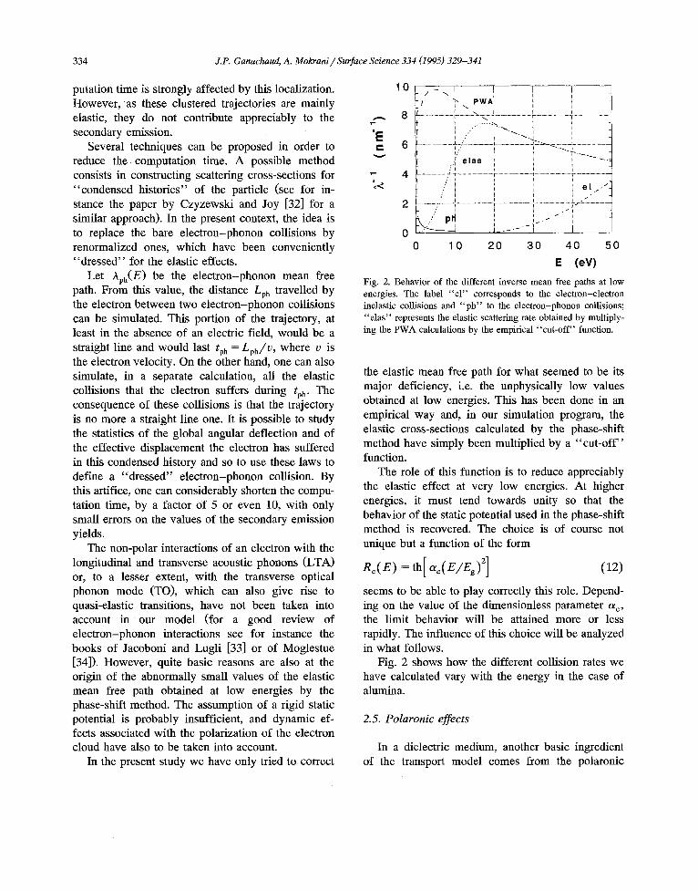
putation time is strongly affected by this localization. However, as these clustered trajectories are mainly elastic, they do not contribute appreciably to the secondary emission.
Several techniques can be proposed in order to reduce the computation time. A possible method consists in constructing scattering cross-sections for "condensed histories" of the particle (see for in- stance the paper by Czyzewski and Joy [32] for a similar approach). In the present context, the idea is to replace the bare electron-phonon collisions by renormalized ones, which have been conveniently "dressed" for the elastic effects.
Let Aph(E) be the electron-phonon mean free path. From this value, the distance Lph travelled by the electron between two electron-phonon collisions can be simulated. This portion of the trajectory, at least in the absence of an electric field, would be a straight line and would last tph = Lph/v, where v is the electron velocity. On the other hand, one can also simulate, in a separate calculation, all the elastic collisions that the electron suffers during tph. The consequence of these collisions is that the trajectory is no more a straight line one. It is possible to study the statistics of the global angular deflection and of the effective displacement the electron has suffered in this condensed history and so to use these laws to define a "dressed" electron-phonon collision. By this artifice, one can considerably shorten the compu- tation time, by a factor of 5 or even 10, with only small errors on the values of the secondary emission yields.
The non-polar interactions of an electron with the longitudinal and transverse acoustic phonons (LTA) or, to a lesser extent, with the transverse optical phonon mode (TO), which can also give rise to quasi-elastic transitions, have not been taken into account in our model (for a good review of electron-phonon interactions see for instance the books of Jacoboni and Lugli [33] or of Moglestue [34]). However, quite basic reasons are also at the origin of the abnormally small values of the elastic mean free path obtained at low energies by the phase-shift method. The assumption of a rigid static potential is probably insufficient, and dynamic ef- fects associated with the polarization of the electron cloud have also to be taken into account.
In the present study we have only tried to correct
10 / ~" PWAI
, , . - . , 8 ................................................ ~ i . . . . . . . . . . . . . . . . . . . . . . 7 . . . . . . . . . . . . . . . . . . . . . . .
'l:: i : ~---.. i e.. 6
.~' e l a s i . . . . . -
" 4 ................... -:;';-i ...................................................... T ............................. ~ .........................
- ' ~ i . ~ ' ~ i
0 . J . . - . - i J 0 1 0 20 30 40 50
E ( e V )
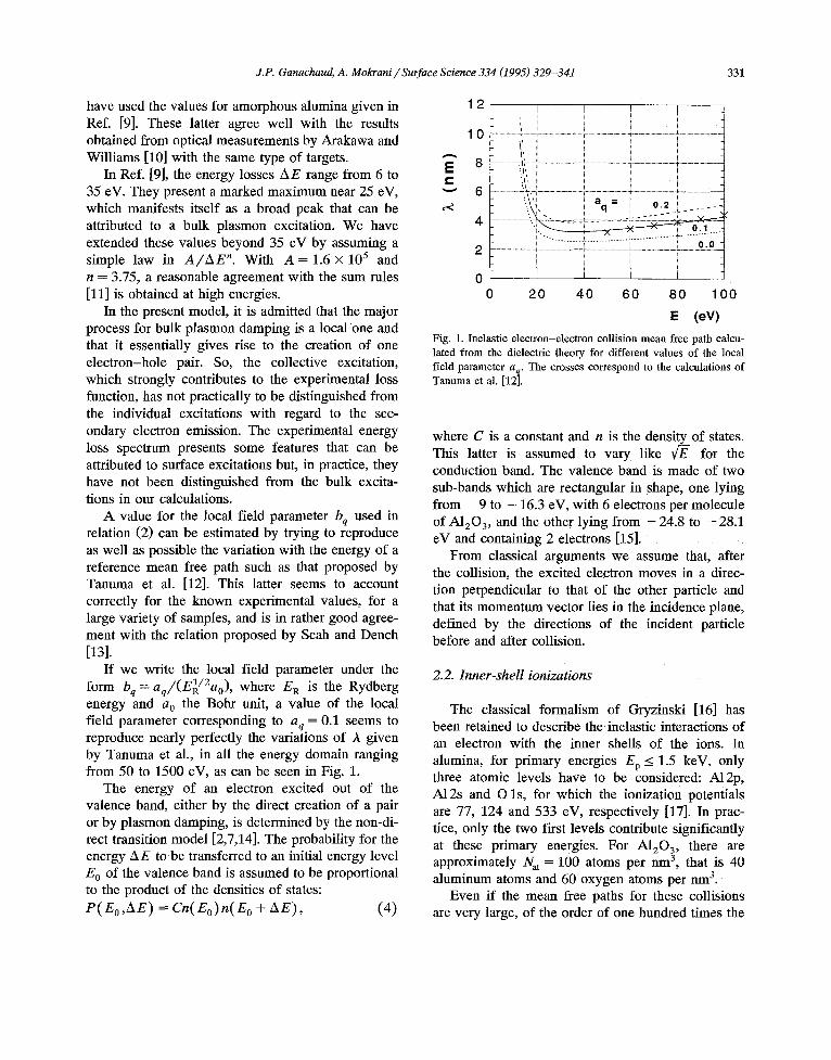
Fig. 2. Behavior of the different inverse mean free paths at low energies. The label "el" corresponds to the electron-electron inelastic collisions and "ph" to the electron-phonon collisions; "elas" represents the elastic scattering rate obtained by multiply- ing the PWA calculations by the empirical "cut-off" function.
the elastic mean free path for what seemed to be its major deficiency, i.e. the unphysically low values obtained at low energies. This has been done in an empirical way and, in our simulation program, the elastic cross-sections calculated by the phase-shift method have simply been multiplied by a "cut-off" function.
The role of this function is to reduce appreciably the elastic effect at very low energies. At higher energies, it must tend towards unity so that the behavior of the static potential used in the phase-shift method is recovered. The choice is of course not unique but a function of the form
Re (E) = th[ a c ( E / E g ) 2] (12)
seems to be able to play correctly this role. Depend- ing on the value of the dimensionless parameter ac, the limit behavior will be attained more or less rapidly. The influence of this choice will be analyzed in what follows.
Fig. 2 shows how the different collision rates we have calculated vary with the energy in the case of alumina.
2.5. Polaronic effects
In a dielectric medium, another basic ingredient of the transport model comes from the polaronic
J.P. Ganachaud, A. Molcrani / Surface Science 334 (1995) 329-341 335
effects. The reader is referred to the review paper by Austin and Mort [35] for instance for a complete presentation. The recent analysis made by Blaise [36] allows an interesting insight into these concepts and permits to clarify their role in space charge physics.
Due to the polarization field it induces around it, an electron can suffer a stabilizing interaction and get trapped in the ionic lattice. It thus behaves like a quasi-particle that can move in the medium, sur- rounded by its polarization cloud. The polaron has generally an important effective mass. The holes created in the valence band due to the inelastic collisions are also subjected to similar effects.
The analysis that will be presented in what fol- lows leads to think that the polaronic effects are essential to understand in a quantitative way the secondary electron emission of insulating targets.
It is probably a huge task, starting from first principles, to integrate all these effects in a simula- tion model. Thus, in the present study, a much more empirical approach has been retained to account for the possibility, for a low energy electron, to get trapped due to this polaronic process. So, the proba- bility per unit of path length, Ptrap(E), of such an event for an electron of energy E has been chosen of the form
Pt~,p(E) = Strap e x p ( - ~/trapE). (13)
The purpose is here to indicate that, rather natu- rally, the weaker its energy is, the more chance the electron has to get trapped and we have arbitrarily chosen an exponential law to account for this. The constant "}/trap limits the energy domain practically concerned by this type of process and the constant St~,p allows to adjust its frequency.
Moreover, we have assumed that, by getting trapped as a polaron, an electron gains a large effec- tive mass and subsequently remains practically local- ized at the trapping site. Its mobility has thus been neglected, even in the presence of an electric field. We have also assumed that the holes created in the valence band had a negligible mobility. All these assumptions obviously deserve a more complete study.
In fact, in an insulating target, the charges can hop from site to site due to thermal excitations or by band conduction. They can also move due to the presence of internal fields. Some of them will recom-
bine. The presence of impurities, either charged or neutral, of defects or more generally of inhomo- geneities of the polarizability in the dielectric medium can be responsible for the existence of potential wells. The existence of such "polarizability defects" can probably be considered as the key concept to
'explain the localization of the polarons and the for- mation of the space charge in an insulating target (see for instance the papers by Le Gressus et al. [37] and by Blaise and Le Gressus [38] for a convincing analysis of all these effects).
The interactions responsible for the trapping and for the detrapping of the charge carriers are influ- enced by the temperature as most of these processes are assisted by phonons. For the moment it seems difficult to introduce explicitly these effects in our model on account of all the other uncertainties which still affect the important mechanisms on which the secondary emission of insulating targets depends.
2.6. Influence of an internal electric field
Simple physical arguments can be proposed to explain how an internal electric field builds up in the insulating material. As the primary electrons pene- trate into the target, they lose energy due to the collisions until they get thermalized, so that their path ends and they get localized. At a certain depth, a negative charge distribution thus sets up. On the other hand, the surface region can charge positively when the secondary current which leaves it exceeds the primary one.
Due to the spatial variation of the charge density with the depth, an internal electric field appears. In actual experiments, the component of the field per- pendicular to the surface can reach several MV/cm. This field will modify the energy and the velocity of the electrons which take part to the transport in the target. The energy gains can be subsequently dissi- pated due to the collisions.
By referring to this scheme, one can represent the variation of the dipolar charge density with the depth z by an analytical expression [39-41]:
p( z ) = P0(1 - z / z * )e -z/z* , (14)
where P0 is the charge density at the surface and z * the depth at which the space charge changes sign.
336 J.P. Ganachaud, A. Mokrani / Surface Science 334 (1995) 329-341
The resulting field can be written as
e z ( z ) = E ° z / z * exp(1 - z / z* ). (15)
In fact, the problem is much more complex and the charge density varies not only with the depth z but also in any direction parallel to the surface, with the distance r from the point of impact of the primary electrons. The field E(r , z ) has thus a radial component Er(r,z) , as well as a longitudinal one Ez(r,z).
In an insulating target submitted to an electron bombardment, the charge and thus the field vary with time. One has also to account for the environ- ment of the target that is for the limit conditions that are imposed to the field (image charges). All these aspects have been analyzed in detail by Cazeaux in Refs. [42,43].
The field depends on the secondary emission, which itself depends on the field. So, to be rigorous, one has to introduce the field in a self-consistent way in the simulation model (see, for instance, Refs. [44,45]).
For the present study, no self-consistency was introduced in our calculations and the various com- ponents of the field have simply been represented by the approximate analytical expressions.
Moreover, to save computational time, the electric field components have been considered as either purely longitudinal or purely radial. For this latter component, we have used the same type of expres- sion as for the longitudinal one:
Er( r) = E ° r / r * exp(1 - r / r *). (16)
In the calculations, E °, E °, z * and r * are consid- ered as parameters which can be varied to check the influence of the electrical field and of its spatial variations on the secondary emission.
From the point of view of the simulation, it has been assumed that the effect of the field was only to modify the energy and velocity of an electron along the path L it travels between two collisions.
2.7. Crossing of the surface potential barrier
Using a classical picture one assumes that, to be emitted when it reaches the free surface of the target,
an electron must have an energy E and a direction a9 (referred to the normal to the surface) such that
ECOS 2 O>__ X, (17)
where X represents the electron affinity of the sam- ple.
Moreover, if the electron reaches the surface out of the emergence cone defined by the aperture angle 20~ = 2arccos[(x /E) l /2] , it is specularly reflected with no energy loss.
For an insulator, the electron affinity X is weak. We lack precise values for alumina, and X probably also varies with the nature of the sample considered. However, from Refs. [39-41], one can estimate that a value of 0.5 eV is correct for amorphous alumina.
3. Results and discussion
3.1. Reference values
There are not many experimental results on the secondary electron emission of metal oxides. How- ever, Kamaya et al. [46] have made a systematic study of the available experimental data for the secondary yield for a large number of insulators. They have proposed a universal relation between the reduced yield 3/Sm and the reduced primary energy Ep/Ern (Em is the value of the primary energy at which the secondary yield reaches its maximum and 6m is this maximum). The values E m = 610 eV and 6 m = 5.4 introduced in this general expression give a good overall agreement with the measurements of Dawson [47] for alumina.
More recently, Saito [48] has also measured the secondary yield for three different targets of alumina ceramics, for a primary energy of 1 keV. The values obtained are 6.0, 5.2 and 6.7. For a sapphire sample, he measured a 6 of 10.1 at the same primary energy.
Our electron-insulator interaction model probably accounts for the main physical processes on which the secondary electron emission of metal oxides depends. However, several parameters appear in the empirical laws we have proposed. The physical meaning of these parameters is quite clear but their values can be precised only by comparing the simu- lation results to the experimental measurements.
J.P. Ganachaud, A. Mokrani / Surface Science 334 (1995) 329-341 337
6 i - - ~ - . . . . !
i
5 ............................. ................. ......................... i ...................................
' i l
4 ................. /~ ................... i i /
3 ................................................ " ............................................. • ............................................
2 - / ..............................................................................................................................................
1 ........................................................... fi ......................................................................................
0 ~ - ~ - - - - ? - - - - - ~ - - , - - o - - - - ~ - - - - -
0 500 1000 1500 E (eV)
P
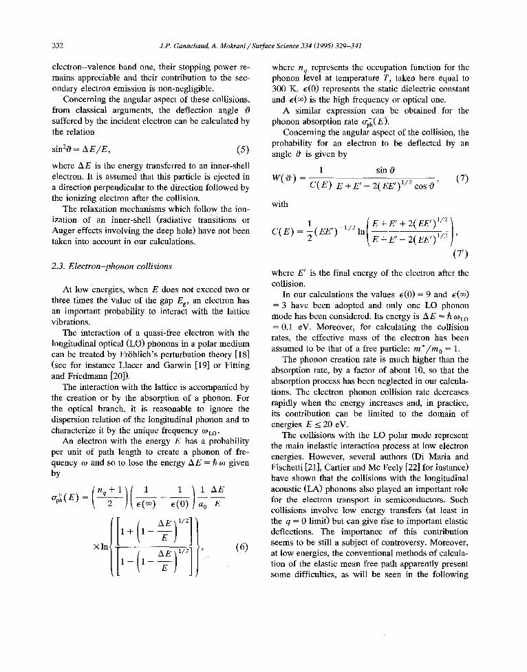
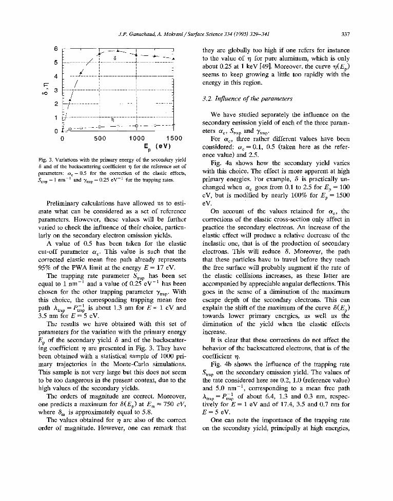
Fig. 3. Variations with the primary energy of the secondary yield 6 and of the backscattering coefficient "q for the reference set of parameters: a c = 0.5 for the correction of the elastic effects, Str~p = 1 nm-1 and ")'trap = 0.25 eV-1 for the trapping rates.
Preliminary calculations have allowed us to esti- mate what can be considered as a set of reference parameters. However, these values will be further varied to check the influence of their choice, particu- larly on the secondary electron emission yields.
A value of 0.5 has been taken for the elastic cut-off parameter ac. This value is such that the corrected elastic mean free path already represents 95% of the PWA limit at the energy E = 17 eV.
The trapping rate parameter Strap has been set equal to 1 nm -1 and a value of 0.25 eV -1 has been chosen for the other trapping parameter Ytrap" With this choice, the corresponding trapping mean free path Atrap-- - 1 - - / ) t rap is about 1.3 nm for E = 1 eV and 3.5 nm for E = 5 eV.
The results we have obtained with this set of parameters for the variation with the primary energy Ep of the secondary yield 6 and of the backscatter- ing coefficient ~7 are presented in Fig. 3. They have been obtained with a statistical sample of 1000 pri- mary trajectories in the Monte-Carlo simulations. This sample is not very large but this does not seem to be too dangerous in the present context, due to the high values of the secondary yields.
The orders of magnitude are correct. Moreover, one predicts a maximum f o r t~(Ep) a t E m = 750 eV, where 6 m is approximately equal to 5.8.
The values obtained for 77 are also of the correct order of magnitude. However, one can remark that
they are globally too high if one refers for instance to the value of r/ for pure aluminum, which is only about 0.25 at 1 keV [49]. Moreover, the curve ~7(Ep) seems to keep growing a little too rapidly with the energy in this region.
3.2. Influence o f the parameters
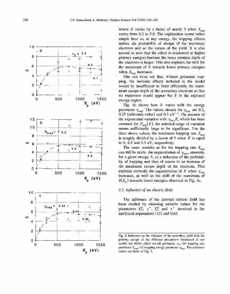
We have studied separately the influence on the secondary emission yield of each of the three param- eters a c, Strap and "rtrap"
For ac, three rather different values have been considered: a c = 0.1, 0.5 (taken here as the refer- ence value) and 2.5.
Fig. 4a shows how the secondary yield varies with this choice. The effect is more apparent at high primary energies. For example, 8 is practically un- changed when a~ goes from 0.1 to 2.5 for Ep = 100 eV, but is modified by nearly 100% for Ep = 1500 eV.
On account of the values retained for cec, the corrections of the elastic cross-section only affect in practice the secondary electrons. An increase of the elastic effect will produce a relative decrease of the inelastic one, that is of the production of secondary electrons. This will reduce 8. Moreover, the path that these particles have to travel before they reach the free surface will probably augment if the rate of the elastic collisions increases, as these latter are accompanied by appreciable angular deflections. This goes in the sense of a diminution of the maximum escape depth of the secondary electrons. This can explain the shift of the maximum of the curve 6(Ep) towards lower primary energies, as well as the diminution of the yield when the elastic effects increase.
It is clear that these corrections do not affect the behavior of the backscattered electrons, that is of the coefficient ~/.
Fig. 4b shows the influence of the trapping rate Strap on the secondary emission yield. The values of the rate considered here are 0.2, 1.0 (reference value) and 5.0 nm -1, corresponding to a mean free path
_ - 1 ~trap- etrap of about 6.4, 1.3 and 0.3 nm, respec- tively for E = 1 eV and of 17.4, 3.5 and 0.7 nm for E = 5 eV.
One can note the importance of the trapping rate on the secondary yield, principally at high energies,
338 J.P. Ganachaud, A. Mokrani / Surface Science 334 (1995) 329-341
10
8
t,,O
6
4
2
0
12
10
8
6
a a =i 2 . 5
. . . . . . . . . . C . i ...............
o ¢
¢ i ................................................. ~ ............... - . ~ ................... i .................... Jl.^.5 . . . . . . . . . . . . . . . . . . .
/ ! 0 ,
I r I I
0 500 1000 1500 E (eV)
P
b ' I ' ~ o ; i o i t
s , .~_= p o2
.................... Q ......................... .a--i ...................... __ ~ ............ - - ~ J ........................................... - , - ~
J- / ~ D 1 " 0 T
2 . . . . . . . . . . . . . . . . . . . . . . . . . . . . . . . . . . . . . . . . . . . . . . . . . . . . . . . . . . . . . . . . . . . . . . . . . . . . . . . . . . . . . . . . . . . . . . . . . . . . . . . . . . . . . . .
0 500 1000 1 5 0 0
E (eV) P
where 6 varies by a factor of nearly 3 when Strap varies from 0.2 to 5.0. The explanation seems rather simple here as, at any energy, the trapping effects reduce the probability of escape of the secondary electrons and so the values of the yield. It is also natural to note that the effect is reinforced at higher primary energies because the mean creation depth of the electrons is larger. This also explains the shift for the maximum of 6 towards lower primary energies when Strap increases.
One can even say that, without polaronic trap- ping, the inelastic effects included in the model would be insufficient to limit efficiently the maxi- mum escape depth of the secondary electrons so that no maximum would appear for 6 in the explored energy region.
Fig. 4c shows how 6 varies with the energy parameter '~trap" The values chosen for ~trap are 0.2, 0.25 (reference value) and 0.3 eV -~. On account of the exponential variation w i t h "ytrapE, which has been assumed f o r etrap(E), the selected range of variation seems sufficiently large to be significant. For the three above values, the maximum trapping rate Str,p is roughly divided by a factor of 5 when E is equal to 8, 6.5 and 5.5 eV, respectively.
The same remarks as for the trapping rate Strap can still be made. An augmentation of "}/trap, amounts, for a given energy E, to a reduction of the probabil- ity of trapping and thus of course to an increase of the maximum escape depth of the electrons. This explains correctly the augmentation of 6 when ')/trap increases, as well as the shift of the maximum of 6(Ep) towards lower energies observed in Fig. 4c.
10
8
6 6 ~
4
2
0
C
Y t r a p = 0 . 3 0 ~ ~ a
............................................ i ............... ~ - - o~.=.~ ..............................................
D ~ ~'/ ~ ° 8 0.20
I I
500 1000 1
E ( e V ) P
3.3. Influence o f an electric f ield
The influence of the internal electric field has been studied by choosing suitable values for the parameters E °, z* , E°r and r* involved in the analytical expressions (15) and (16).
i00
Fig. 4, Influence on the variation of the secondary yield with the primary energy of the different parameters introduced in our model: (a) elastic effect cut-off parameter o~c; (b) trapping rate parameter Strap; (C) trapping energy parameter Ytrap" The reference values are those of Fig. 3.
J.P. Ganachaud, A. Mokrani / Surface Science 334 (1995) 329-341 339
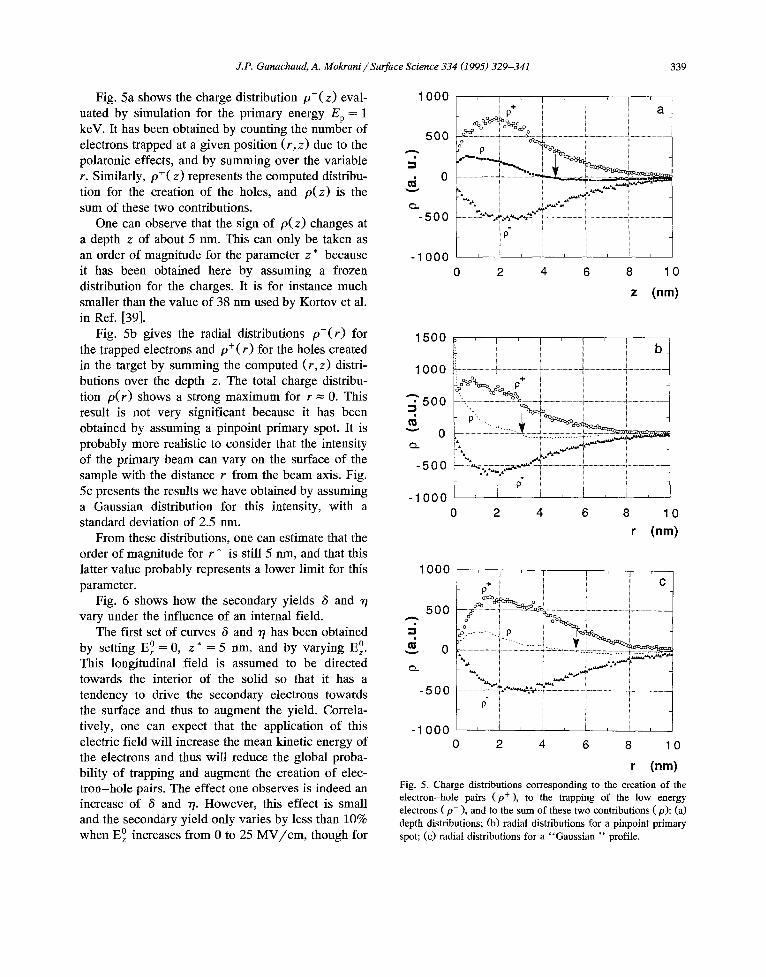
Fig. 5a shows the charge distribution p-(z) eval- uated by simulation for the primary energy Ep = 1 keV. It has been obtained by counting the number of electrons trapped at a given position (r,z) due to the polaronic effects, and by summing over the variable r. Similarly, p+(z) represents the computed distribu- tion for the creation of the holes, and p(z) is the sum of these two contributions.
One can observe that the sign of p(z) changes at a depth z of about 5 nm. This can only be taken as an order of magnitude for the parameter z * because it has been obtained here by assuming a frozen distribution for the charges. It is for instance much smaller than the value of 38 nm used by Kortov et al. in Ref. [39].
Fig. 5b gives the radial distributions p-(r) for the trapped electrons and p+(r ) for the holes created in the target by summing the computed (r,z) distri- butions over the depth z. The total charge distribu- tion p(r) shows a strong maximum for r = 0. This result is not very significant because it has been obtained by assuming a pinpoint primary spot. It is probably more realistic to consider that the intensity of the primary beam can vary on the surface of the sample with the distance r from the beam axis. Fig. 5c presents the results we have obtained by assuming a Gaussian distribution for this intensity, with a standard deviation of 2.5 nm.
From these distributions, one can estimate that the order of magnitude for r * is still 5 rim, and that this latter value probably represents a lower limit for this parameter.
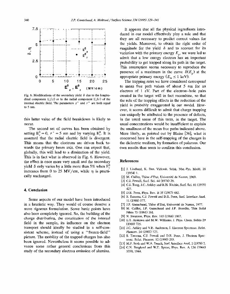
Fig. 6 shows how the secondary yields 6 and ~7 vary under the influence of an internal field.
The first set of curves 6 and ~7 has been obtained by setting E ° = 0, z * = 5 rim, and by varying E °. This longitudinal field is assumed to be directed towards the interior of the solid so that it has a tendency to drive the secondary electrons towards the surface and thus to augment the yield. Correla- tively, one can expect that the application of this electric field will increase the mean kinetic energy of the electrons and thus will reduce the global proba- bility of trapping and augment the creation of elec- tron-hole pairs. The effect one observes is indeed an increase of 8 and r/. However, this effect is small and the secondary yield only varies by less than 10% when E ° increases from 0 to 25 MV/cm, though for
1 0 0 0
5OO
0
o , .
- 5 0 0
- 1 0 0 0
I ' I
i a
~. .................. i ................ ~-.-.-i ..................................................................................... ? p i i i • - . . . . . . . . i -
.............. ~*~ ; ,4 '~ , ' , '~ ,~ ' - . . - - i ............................. 4 ............................... i .............................
, , i , i , ,
0 2 4 6 8 10
z ( r i m )
1 5 0 0
1 0 0 0
'•'500 " " 0
- 5 0 0
- 1 0 0 0
b
., ~ q~q=oOo - - . : ~ : . . . . . . . . . . . . . . . . . . . . . 4 . . . . . . . . . . . . o . . . . . . . . . . . } . . . . . . . . . . . . . . . . . . . . . . . . . . 1 . . . . . . . . . . . . . . . . . . . . . . . . . . ~ . . . . . . . . . . . . . . . . . . . . . . . . .
| - ? ~ i .................... [.[~ .;;.:-:.:. :.:.:.:-: ::-:.: : . : - : : ~
..... "~'::~:;~ . . . . . . . i ..................................................................................
0 2 4 6 8 10
r ( n m )
1 0 0 0 ' p + . . . . C
. - . 5 o o FJ .............. i .................... ..................... ............................ T ......................
= i . . . . . . . . . . . . i -
i . , ~ , . ~ ' - " "
- 5 0 0 ................... ~ % ~ ' ~ - - ~ ' ~ ........................................................................... p i
- 1 0 0 0 , i . . . .
0 2 4 6 8 10
r (nm) Fig. 5. Charge distributions corresponding to the creation of the electron-hole pairs ( p + ) , to the trapping of the low energy electrons ( p - ), and to the sum of these two contributions ( p): (a) depth distributions; (b) radial distributions for a pinpoint primary spot; (c) radial distributions for a "Gaussian " profile.
340 J.P. Ganachaud, A. Mokrani / Surface Science 334 (1995) 329-341
7 . 5 , , , , , , , , J , , i [ L , , , i , ~ , ,
_ , ~ . . . . . . . ~ . . . . . . . ~ . . . . . . . ~ . . . . . .
. . . . . . . . . . . . . . . . . . . . . . . . . ~ . . . . . . . . . . . . . . . . . . . . . . . . . . . . . , . . . . . . . . ~ . . . . . . . . . . . . . . . . . . . . . . . .
~-- . . . . . . . E o ! Z
~:~ • E 0 ! r
2 . 5 ...................................................................................................................................................
0 -;-, T ~',-;-, . 'Y ,-~-, . ~ ,-i-, : ? ' , - i - : 0 5 1 0 1 5 2 0 2 5
E" E ° , ( M V / c m ) Z r
Fig. 6. Modifications of the secondary yield 6 due to the longitu- dinal component Ez(Z) or to the radial component Er(r) of the internal electric field. The parameters z * and r * are both equal to 5 nm.
this latter value of the field breakdown is l ikely to o c c u r .
The second set of curves has been obtained by setting E°z = 0, r * = 5 nm and by varying E °. It is assumed that the radial electric field is divergent. This means that the electrons are driven back to- wards the primary beam axis. One can expect that, globally, this will lead to a diminution of the yield. This is in fact what is observed in Fig. 6. However, the effect is once more very small and the secondary yield 6 only varies by a little more than 5% when E ° increases from 0 to 25 M V / c m , while r/ is practi- cally unchanged.
4. Conc lus ion
Some aspects of our model have been introduced in a heuristic way. They would of course deserve a more rigorous formulation. Some basic points have also been completely ignored. So, the building of the charge distribution, the constitution of the internal field in the sample, its influence on the electron transport should ideally be studied in a self-con- sistent scheme, instead of using a " f rozen- f i e ld" picture. The mobil i ty of the trapped charges has also been ignored. Nevertheless it seems possible to ad- vance some rather general conclusions from this study of the secondary electron emission of alumina.
It appears that all the physical ingredients intro- duced in our model effectively play a role and that they are all necessary to predict correct values for the yields. Moreover, to obtain the right order of magnitude for the yield 6 and to account for its variation with the primary energy Ep, we were led to admit that a low energy electron has an important probabil i ty to get trapped along its path in the target. This assumption seems necessary to reproduce the presence of a maximum in the curve 6(Ep) at the appropriate primary energy ( E m ~ i keV).
The trapping rates we have considered correspond to mean free path values of about 5 nm for an electron of 1 eV. Part of the e lec t ron-hole pairs created in the target wil l in fact recombine, so that the role of the trapping effects in the reduction of the yield is probably exaggerated in our model. How- ever, it seems difficult to admit that charge trapping can uniquely be attributed to the presence of defects, in the usual sense of this term, in the target. The usual concentrations would be insufficient to explain the smallness of the mean free paths indicated above. More likely, as pointed out by Blaise [36], what is concerned here is the self-trapping of the charges in the dielectric medium, by formation of polarons. Our own results thus seem to confirm this conclusion.
R e f e r e n c e s
[1] J. Lindhard, K. Dan. Vidensk, Selsk. Mat.-Fys. Medd. 28 (1954) 1.
[2] M. Cailler, ThOse d'Etat, Universit6 de Nantes, 1969. [3] C.J. Powell, Surf. Sci. 44 (1974) 29. [4] C.J. Tung, J.C. Ashley and R.H. Ritchie, Surf. Sci. 81 (1979)
427. [5] D.R. Penn, Phys. Rev. B 35 (1987) 482. [6] S. Tanuma, C.J. Powell and D.R. Penn, Surf. Interface Anal.
11 (1988) 577. [7] J.P. Ganachaud, ThOse d'Etat, Universit6 de Nantes, 1977. [8] M. Cailler, J.P. Ganachaud and J.P. Bourdin, Thin Solid
Films 75 (1981) 181. [9] N. Swanson, Phys. Rev. 165 (1968) 1067.
[10] E.T. Arakawa and M.W. Williams, J. Phys. Chem. Solids 29 (1968) 735.
[11] J.C. Ashley and V.E. Anderson, J. Electron Spectrosc. Relat. Phenom. 24 (1981) 127.
[12] S. Tanuma, C.J. Powell and D.R. Penn, J. Electron Spec- trosc. Relat. Phenom. 52 (1990) 285.
[13] M.P. Seah and W.A. Dench, Surf. Interface Anal. 1 (1979) 2. [14] C.N. Berglund and W.E. Spicer, Phys. Rev. A 136 (1964)
1030, 1044.
J.P. Ganachaud, A. Mokrani / Surface Science 334 (1995) 329-341 341
[15] Y.N. Xu and W.Y. Ching, Phys. Rev. B 43 (1991) 4461. [16] M. Gryzinski, Phys. Rev. A 138 (1965) 305, 322, 336. [17] J.A. Bearden and A.F. Burr, Rev. Mod. Phys. 39 (1967) 125. [18] H. Frdhlich, Adv. Phys. 3 (1954) 325. [19] J. Llacer and E.L Garwin, J. Appl. Phys. 40 (1969) 2766,
2776. [20] H.J. Fitting and J.U. Friedmann, Phys. Status Solidi (a)69
(1982) 349. [21] D.J. Di Maria and M.V. Fischetti, J. Appl. Phys. 64 (1988)
4683. [22] E. Cartier and F.R. Mc Feely, Phys. Rev. B 44 (1991) 10689. [23] M. Cailler and J.P. Ganachaud, Scanning Microsc. Suppl. 4
(1990) 81. [24] S. Ichimura and R. Shimuzu, Surf. Sci. 112 (1981) 386. [25] A. Jablonski, J. Gryko, J. Kraeer and S. Tougaard, Phys.
Rev. B 39 (1989) 61. [26] J. Devooght, J.C. Dehaes, A. Dubus, M. Cailler and J.P.
Ganachaud, Vol. 122 of Springer Tracts in Modem Physics (Springer, Berlin, 1991) p. 67.
[27] J.B. Pendry, Low Energy Electron Diffraction (Academic Press, New York, 1974).
[28] R.A. Bonham and T.G. Strand, J. Chem. Phys. 39 (1963) 2200.
[29] D. Jousset, Th~se de Doctorat de l'Universit6 Paris VI, 1987. [30] B.P. Nigam, M.K. Sundarisan and T.Y. Wu, Phys. Rev. 115
(1959) 491. [31] I. Adesida, R. Shimizu and T.E. Everhart, Appl. Phys. Lett.
33 (1978) 849. [32] Z. Czyzewski and D.C. Joy, J. Microsc. 156 (1989) 285. [33] C. Jacoboni and P. Lugli, The Monte Carlo Method for
Semiconductor Device Simulation, in: Computational Micro- electronics, Ed. S. Selberherr (Springer, Berlin, 1989).
[34] C. Moglestue, Monte Carlo Simulation of Semiconductor Devices (Chapman & Hall, London, 1993) . . . . .
[35] I.G. Austin and N.F. Mott, Adv. Phys. 18 (1969) 4]. [36] G. Blaise, Confdrence Interdisciplinaire sur les Didlectriques,
Antibes, 1992, in: Le Vide-Les Couches Minces, Suppl. 260 (1992) 1, 417.
[37] C. Le Gressus, F. Valin, H. Gautier, J.P. Duraud, J. Cazaux and H. Okuzumi, Scanning 12 (1990) 203.
[38] G. Blaise and C. Le Gressus. J. Appl. Phys. 69 (1991) 6334. [39] V. Kortov, V. Isakov, A. GaprindoshviLy, H.J. Fitting, H.
Glaefeke and W. Wild, Phys. Status Solidi (a)54 (1979) 633. [40] Y. Watanabe, Y. Takemoto, T. Kubozoe and T. Mukoyama,
Phys. Status Solidi (a)61 (1980) 221. [41] H. Lanteri, P. Rostaing and R. Bindi, Phys. Status Solidi
(b)149 (1988) 203. [42] J. Cazaux, J. Appl. Phys. 59 (1986) 1418. [43] J. Cazaux, Conference Interdisciplinaire sur les Didlectriques,
Antibes, 1992, in: Le Vide-Les Couches Minces, Suppl. 260 (1992) 36.
[44] H.J. Fitting, H. Glaefeke, W. Wild, M. Franke and W. Miiller, Exp. Tech. Phys. 27 (1979) 13.
[45] R. Renoud, E. Vicario and N. Rosenberg, Confdrence Inter- disciplinaire sur les Didlectriques, Antibes, 1992; Le Vide- Les Couches Minces, Suppl. 260 (1992) 305.
[46] K. Kanaya, S. Ono and F. Ishigaki, J. Phys. D: Appl. Phys. 11 (1978) 2425.
[47] P.H. Dawson, J. Appl. Phys. 37 (1966) 3644. [48] Y. Saito, Confdrence Interdisciplinaire sur les Didlectriques,
Antibes, 1992, in: Le Vide-Les Couches Mincesm, Suppl. 260 (1992) 385.
[49] I.M. Bronshtejn and B.S. Frajman, Secondary Electron Emis- sion (Nauka, Moscow, 1969) [in Russian].


![[Draft] Secondary Noise Screening Process Guide · Secondary Noise Screening Process Guide . September 2016, Version 4.0 (Draft) Cette publication hautement spécialisée Secondary](https://img.pdfslide.fr/doc/110x75/5ed2ce219c95614861233479/draft-secondary-noise-screening-process-secondary-noise-screening-process-guide.jpg)