Embed Size (px)
Citation preview
THIN FILMS THERMAL CONDUCTIVITY VERSUS
SUBSTRATE SURFACE ROUGHNESS
Andrzej KUSIAK1, Jean-Luc BATTAGLIA
Laboratoire inter établissement ‘TRansferts Ecoulements Fluides Energétique’, UMR 8508,
Ecole Nationale Supérieure d’Arts et Métiers, Esplanade des Arts et Métiers, 33405 Talence
Cedex, France.
Email : [email protected]
Tel: +33 5 56 84 54 21
Fax: +33 5 56 84 54 36
Sonia GOMEZ, Jean-Pierre MANAUD, Yann LEPETITCORPS
Institut de Chimie de la matière Condensée de Bordeaux, UMR, 87 Avenue du Docteur
Schweitzer 33608 Pessac cedex.
1 Corresponding author
Abstract
The thermal conductivity and the interface thermal contact resistance of four different
thickness CuO films, obtained by PVD on a tungsten carbide substrate were investigated. The
periodic photothermal experiment based on infrared measurement was developed. According
to the knowledge of the substrate thermophysical properties the gain between the thermal
perturbation and the response was used as the experimental data. The results show the
dependence of the thermal conductivity on the film thickness. The scanning electron
microscopy observations present strong anisotropy and columnar structure of the deposits.
Moreover, the chemical composition of films was tested. The presence of cobalt diffused
from the substrate was revealed, and similar composition for each film was found.
Keywords: Thin Film, Thermal Conductivity, Radiative Photothermal Experiment, Thermal
Contact Resistance
Introduction
The thermal conductivity estimation of thin solid films of sub micrometric thickness on the
form of a coating is well treated in the literature. There exist different experimental
approaches all based on the front face technique. It consists in measuring the temperature at
the location of the thermal disturbance that is a heat flux (see figure 1). The 3-ω technique is
perhaps the simplest experimental method [1]. It consists in deposing an Au layer on the
deposit whose thermal conductivity is unknown. A periodic current passes through the Au
layer that induced Joule effect and heat transfer in the deposit and the substrate. Given that the
Au electrical resistance depends on the temperature, the Au layer is used as the heater and as
the thermal sensor. Indeed, this resistance can be measured by inserting the Au layer in a
Wheatstone bridge. A comparable method is used in [2] but its configuration differs from the
previous one by focusing a pico-second laser beam on the Au layer that is covered by a
constant current. This technique permits exploring highest frequencies and lead to estimate
the thermal conductivity as well of the thermal diffusivity of the deposit. In the experimental
configuration developed by [3], the surface temperature measurement is reached using the
thermo-reflectance technique. The Au layer is well appropriate for such an experiment given
it offers a very interesting thermo reflection coefficient. As previously, this experiment can
also lead estimating the thermal diffusivity. Furthermore, surface temperature can be obtained
using the photothermal infrared radiometry technique. Obviously in that case, the Au layer
disappears and heating is obtained by focusing a laser beam on the material.
Two classical heat flux waveforms are used in such thermal characterization experiments: the
periodic one and the impulse one. As presented in [4] and [5], each approach has its own
advantages and drawbacks. It must be also cited the use of an intermediate approach based on
the use of a random heat flux [6]. In practice, the impulse technique requires only one
experiment as the periodic method requires an experiment for each explored frequency.
Nevertheless, this last method leads to the best results in terms of reliability and estimated
parameters confidence domains. A sensitivity study is performed in order to precisely define
the limits of the frequency domain according to the parameters that will be estimated (thermal
conductivity and diffusivity).
Whatever the choice of the experimental technique and heat flux disturbance, the result is the
same: the thermal conductivity of the thin layer strongly varies according to its thickness.
This conductivity is all the more small as the thickness is itself small. Cahill and Lee [1] and
showed this phenomenon on deposits of SiO2, TiO2, Al2 O3, HfO2 and MgO. Orain et al. [2]
find a comparable tendency for a Zr02 film. Bhusari et al. [7] obtain also this decrease for an
aluminium deposit, of which the thickness varies from 0.5 to 2.5 µm, on a silicon and copper
substrate. On the contrary, Langer et al. [8] show that the thermal conductivity of a nickel
film on a quartz substrate does not vary according to the thickness.
Several reasons are called upon to explain this variation of conductivity according to the
thickness. First of all, when metal layer thickness is lower than 10-100 nm, the mean free path
of the carriers (phonons and electrons) does not make possible the definition of thermal
conductivity within the meaning of the Fourrier law. In that case, it is necessary to carry out a
model of molecular dynamics scale, and thermal conductivity is that of the lattice [9] [10]. For
larger thicknesses, the variation of conductivity comes from the considerable influence of the
deposit-substrate interface. The imperfect contact between materials is modelled in the form
of a thermal contact resistance. This resistance is related to many parameters but in fact the
parameters (temperature, pressure) related to the process of deposition (PVD, CVD) have the
most significant contribution. It was shown for a long time the influence of the deposition
temperature on the arrangement of the constitutive particles of the layer and on its density
[11]. In the same way, particles column-like arrangement is found at critical temperatures. In
that case, it would be judicious to consider an anisotropic thermal conductivity, in any event
incomparable with that of the bulk material. Lastly, when the substrate is not chemically any
more neutral with respect to the deposit, one must take into account species diffusion
phenomenon with the deposit-substrate interface.
The objective of this work is to show the relation between the thermal conductivity of the
deposit, its structure, its chemical composition and the surface roughness of the substrate. For
that, our step is built around the characterization of a CuO deposit which one varied the
thickness. The coating is deposited by PVD on a WC-Co9% substrate. It has an average
roughness (~300 nm) and cobalt diffuses rather easily in the deposit at the time of the
deposition process.
The total surface emissivity of the CuO is close to 0.8 in the 0-100°C temperature range [12].
Such a feature improves incident radiation absorption and infrared radiation emissivity.
Thereby, the experimental method for the thermal conductivity estimation is based on the
periodic photothermal infrared radiometry.
Modulated photothermal IR radiometry experiment
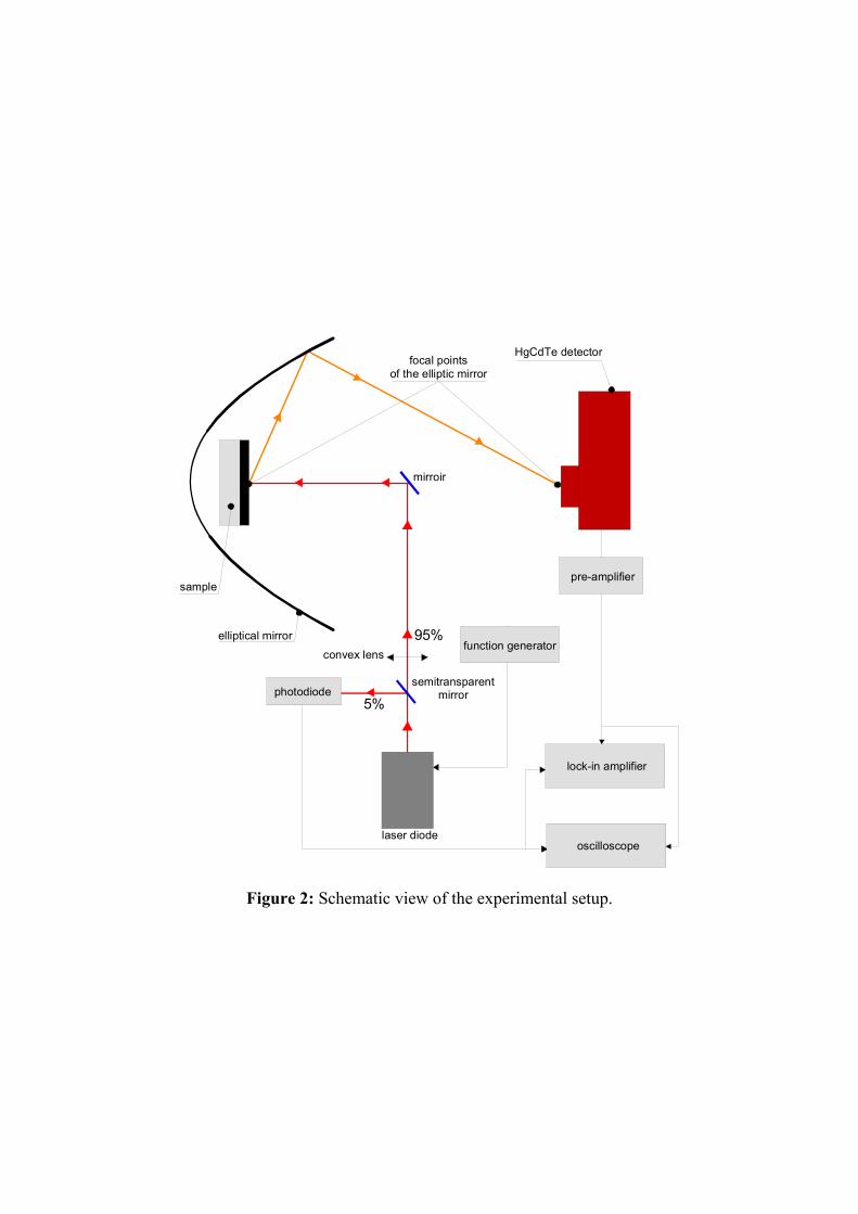
The schematic view of the measurement arrangement is shown in figure 2. The system is
composed of two parts: the sample excitation and the thermal response measurement. The
thermal excitation is generated on the deposit front face from a laser diode of 808 nm
wavelength and 5 W maximal power. The laser is modulated directly from its driver using
sinusoidal signal from the frequency function generator. Such external modulation range is up
to 20 kHz. Focused on the mirror by a convex lens the laser beam is redirected
perpendicularly to the face of the studied sample. The laser beam has a Gaussian profile as
specified from the constructor. A very fast photodiode is used to measure the reference signal
in order to avoid the phase lag due to the laser diode driver.
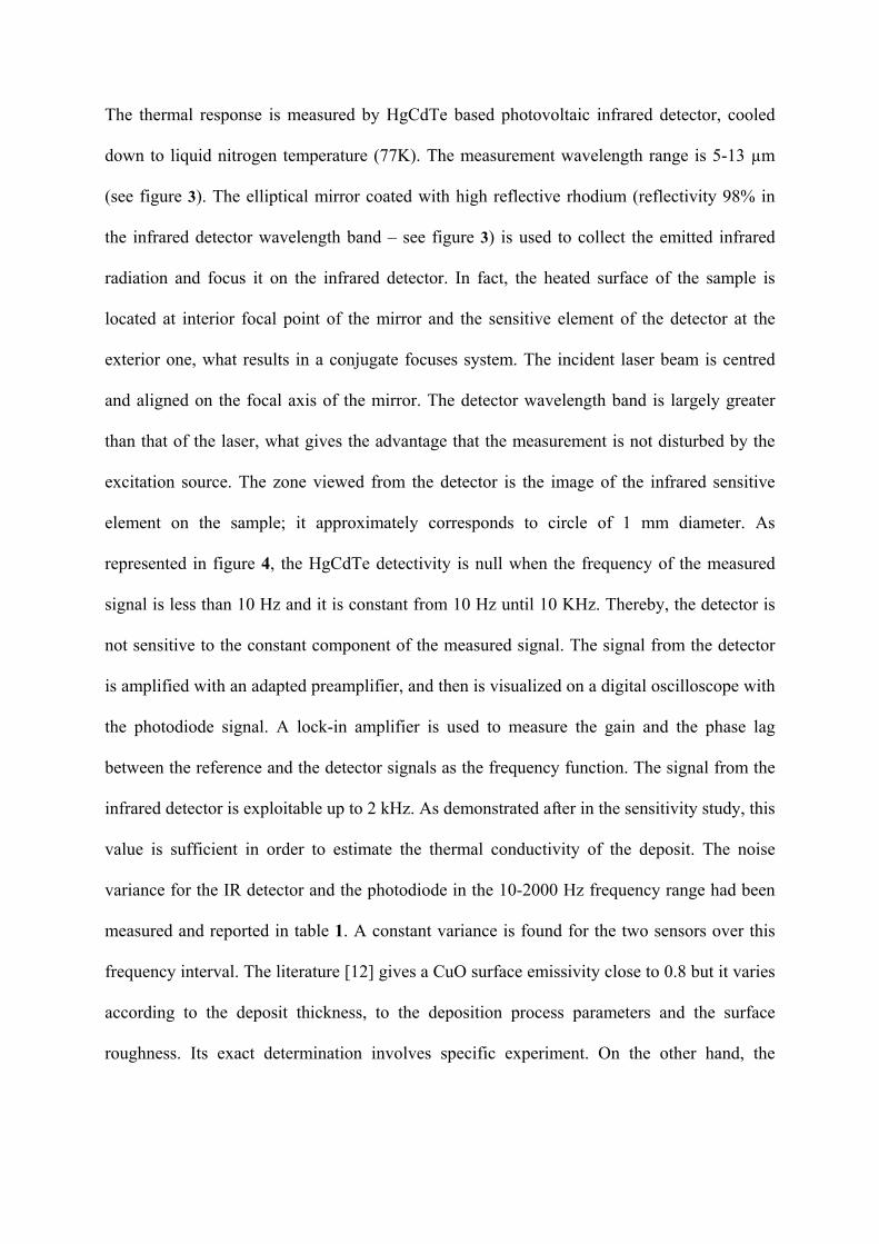
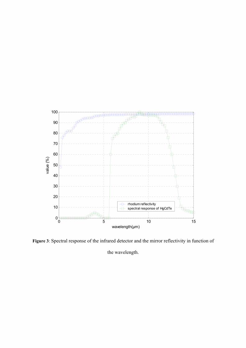
The thermal response is measured by HgCdTe based photovoltaic infrared detector, cooled
down to liquid nitrogen temperature (77K). The measurement wavelength range is 5-13 µm
(see figure 3). The elliptical mirror coated with high reflective rhodium (reflectivity 98% in
the infrared detector wavelength band – see figure 3) is used to collect the emitted infrared
radiation and focus it on the infrared detector. In fact, the heated surface of the sample is
located at interior focal point of the mirror and the sensitive element of the detector at the
exterior one, what results in a conjugate focuses system. The incident laser beam is centred
and aligned on the focal axis of the mirror. The detector wavelength band is largely greater
than that of the laser, what gives the advantage that the measurement is not disturbed by the
excitation source. The zone viewed from the detector is the image of the infrared sensitive
element on the sample; it approximately corresponds to circle of 1 mm diameter. As
represented in figure 4, the HgCdTe detectivity is null when the frequency of the measured
signal is less than 10 Hz and it is constant from 10 Hz until 10 KHz. Thereby, the detector is
not sensitive to the constant component of the measured signal. The signal from the detector
is amplified with an adapted preamplifier, and then is visualized on a digital oscilloscope with
the photodiode signal. A lock-in amplifier is used to measure the gain and the phase lag
between the reference and the detector signals as the frequency function. The signal from the
infrared detector is exploitable up to 2 kHz. As demonstrated after in the sensitivity study, this
value is sufficient in order to estimate the thermal conductivity of the deposit. The noise
variance for the IR detector and the photodiode in the 10-2000 Hz frequency range had been
measured and reported in table 1. A constant variance is found for the two sensors over this
frequency interval. The literature [12] gives a CuO surface emissivity close to 0.8 but it varies
according to the deposit thickness, to the deposition process parameters and the surface
roughness. Its exact determination involves specific experiment. On the other hand, the
incident heat flux can not be easily measured. Thus, the chosen available measurable
quantities are the voltage at the HgCdTe sensor and at the photodiode.
Heat transfer modelling
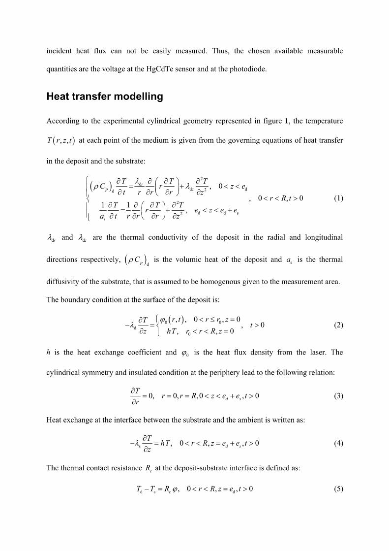
According to the experimental cylindrical geometry represented in figure 1, the temperature
( ), ,T r z t at each point of the medium is given from the governing equations of heat transfer
in the deposit and the substrate:
( )
2d
d d2d
2
d d s2s
, 0, 0 , 0
1 1 ,
rp z
T T TC r z et r r r z
r R tT T Tr e z e e
a t r r r z
λρ λ ∂ ∂ ∂ ∂ = + < < ∂ ∂ ∂ ∂ < < >
∂ ∂ ∂ ∂ = + < < + ∂ ∂ ∂ ∂
(1)
drλ and dzλ are the thermal conductivity of the deposit in the radial and longitudinal
directions respectively, ( )dpCρ is the volumic heat of the deposit and sa is the thermal
diffusivity of the substrate, that is assumed to be homogenous given to the measurement area.
The boundary condition at the surface of the deposit is:
( )0 0d
0
, , 0 , 0, 0
, , 0r t r r zT t
z hT r r R zϕ
λ < ≤ =∂
− = >∂ < < = (2)
h is the heat exchange coefficient and 0ϕ is the heat flux density from the laser. The
cylindrical symmetry and insulated condition at the periphery lead to the following relation:
0, 0, ,0 , 0d sT r r R z e e tr
∂= = = < < + >
∂ (3)
Heat exchange at the interface between the substrate and the ambient is written as:
s , 0 , , 0d sT hT r R z e e tz
λ ∂− = < < = + >
∂ (4)
The thermal contact resistance cR at the deposit-substrate interface is defined as:
d s d, 0 , , 0cT T R r R z e tϕ− = < < = > (5)
Finally, the initial condition is:
0, 0 ,0 d sT r R z e e= ≤ ≤ ≤ ≤ + (6)
Applying the Fourrier transform, versus the time variable, on the temperature and the heat
flux density lead to:
( ) ( ) ( ) ( )0 0
, , , , d , , , dj t j tr z j T r z t e t r j r t e tω ωθ ω ψ ω ϕ∞ ∞
− −= =∫ ∫ (7)
Thereby, relations (1) to (6) become:
( )
2d
d d2d
2
d d s2s
, 0, 0
1 ,
rp zC s r z e
r r r zr R
s r e z e ea r r r z
λ θ θρ θ λ
θ θθ
∂ ∂ ∂ = + < < ∂ ∂ ∂ < <∂ ∂ ∂ = + < < + ∂ ∂ ∂
(8)
0 0
0
, 0 , 0, , 0d
r r zh r r R zzψθλθ
< ≤ =∂− = < < =∂
(9)
0, 0, ,0 d sr r R z e erθ∂= = = < < +
∂ (10)
, 0 ,s d sh r R z e ezθλ θ∂
− = < < = +∂
(11)
d s d, 0 ,cR r R z eθ θ ψ− = < < = (12)
According to the cylindrical symmetry, one can apply the Hankel transform on the
temperature and the heat flux density, versus the radial coordinate, as:
( ) ( ) ( )00
, , , , dR
z s r z s r J r rθ α θ α= ∫ , ( ) ( ) ( )00
, , dR
s r s r J r rψ α ψ α= ∫ (13)
Thus, relations (8) to (12) become:
( )
22
d d d2d
22
d d s2s
, 0
,
p r zC s z ez
s e z e ea z
θρ θ α λ θ λ
θθ α θ
∂=− + < < ∂
∂ =− + < < +
∂
(14)
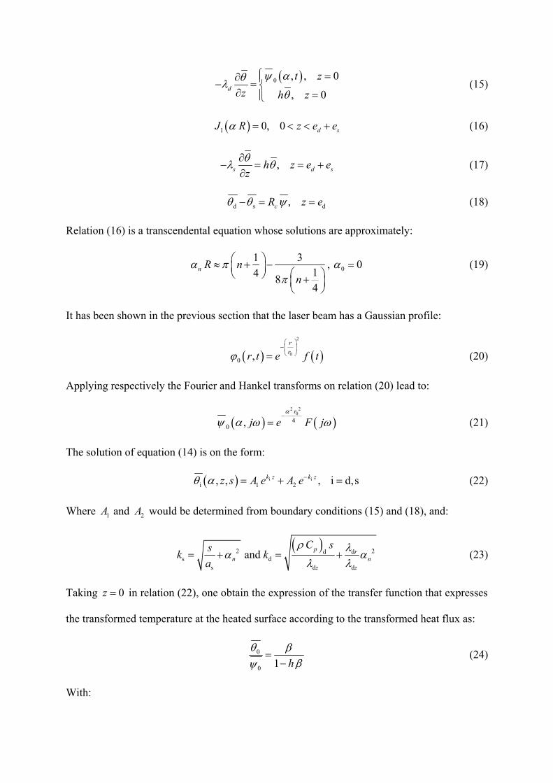
( )0 , , 0
, 0d
t zz h z
ψ αθλθ
=∂ − = ∂ = (15)
( )1 0, 0 d sJ R z e eα = < < + (16)
,s d sh z e ezθλ θ∂
− = = +∂
(17)
d s d,cR z eθ θ ψ− = = (18)
Relation (16) is a transcendental equation whose solutions are approximately:
1 314 84
n R nn
α ππ
≈ + − +
, 0 0α = (19)
It has been shown in the previous section that the laser beam has a Gaussian profile:
( ) ( )2
00 ,
rrr t e f tϕ
− = (20)
Applying respectively the Fourier and Hankel transforms on relation (20) lead to:
( ) ( )2 2
04
0 ,r
j e F jα
ψ α ω ω−
= (21)
The solution of equation (14) is on the form:
( ) i ii 1 2, , , i d,sk z k zz s A e A eθ α −= + = (22)
Where 1A and 2A would be determined from boundary conditions (15) and (18), and:
( )2 2d d
s ds d d
and p rn n
z z
C ssk ka
ρ λα αλ λ
= + = + (23)
Taking 0z = in relation (22), one obtain the expression of the transfer function that expresses
the transformed temperature at the heated surface according to the transformed heat flux as:
0
0 1 hθ β
βψ=
− (24)
With:
A h BC h D
β +=
+ (25)
And:
( ) ( ) ( ) ( ) ( )
( ) ( ) ( ) ( ) ( )
( ) ( ) ( ) ( )( ) ( )
( )
d dd d d d s s s s
d d
s s d dd d d d s s
s s d d
d d d d s s d d d d d d s s s s
d d d d
sinhcosh cosh cosh sinh
sinh sinhcosh cosh cosh
sinh cosh sinh cosh sinh
sinh cosh
s s c
c
c
c
k eA k e k e k e R k k e
k
k e k eB k e k e R k e
k k
C k k e k e k k e R k e k k e
D k k e R k
λλ
λ λ
λ λ λ
λ
= + +
= + +
= + +
= + ( )( ) ( ) ( ) ( )d dd d s s d d s s
s s
cosh sinh sinhke k e k e k ek
λλ
+
(26)
Using the thermoelectric analogy gives more insight on the heat transfer transient behaviour
as represented on the top of figure 5. dZ and sZ respectively denote the deposit and substrate
impedances.
Low frequency behaviour and sensitivity study
At low heat flux frequencies, 2d df a e<< , the deposit is viewed as a thermal resistance and
the transfer function can be largely simplified given that parameters A, B, C and D of relation
(26) become:
( ) ( )( ) ( )
( )( )
s s d s s s s
s sd s s
s s
s s s s
s s
cosh sinh
sinhcosh
sinh
cosh
A k e R k k e
k eB R k e
kC k k e
D k e
λ
λλ
= + = + = =
(27)
In this relation the thermal resistance dR is expressed according to the thermal conductivity in
the longitudinal direction and the thickness of the deposit and the thermal contact cR as:
cdd
d ~ Ree
Rdzdz
+==λλ
(28)
The equivalent electrical scheme is represented at the bottom of figure 5.
Applying the inverse Hankel transform on relation (24) lead to:
( ) ( )( )
( )2 2
00 4
0 221 0
2,
1
n rNn
n n
J rr j e F j
hR J R
αα βθ ω ωβα
−
=
= − ∑ (29)
The average temperature on the measurement area is:
( ) ( )0 020
2 , dmr
m
j r j r rr
θ ω θ ω= ∫ (30)
With respect to relation (29), one obtains an analytical expression of the average temperature
on the measurement area as:
( )( )
( )( )
( )
2 20
2 20
2
4
1
0
1 422
1 0
2 , 01
4, 0
1
n
n
rN
n m
rNn m
n m n n
e F j nr R h
jJ r
e F j nhr R J R
α
α
β ωβ
θ ωα β ω
βα α
−
=
−
=
= − =
> −
∑
∑ (31)
That can be written on the transfer functional form: ( ) ( ) ( )0 j Z j F jθ ω ω ω= (32)
We use the classical definition of the gain of the transfer function as:
( ) ( )1020 logG j Z jω ω= (33)
As said in the previous section, the heat flux and the temperature can not be estimated
accurately. The measurement of the photodiode and the infrared detector voltage leads to the
gain proportional to that between the heat flux and the temperature. The sensitivity study for
the gain evolution versus the frequency and the thermal properties permits to overcome this
drawback. In fact the low frequency behaviour of the deposit-substrate system for a large
thermal conductivity range is identical as the uncoated substrate. Such behaviour permits to
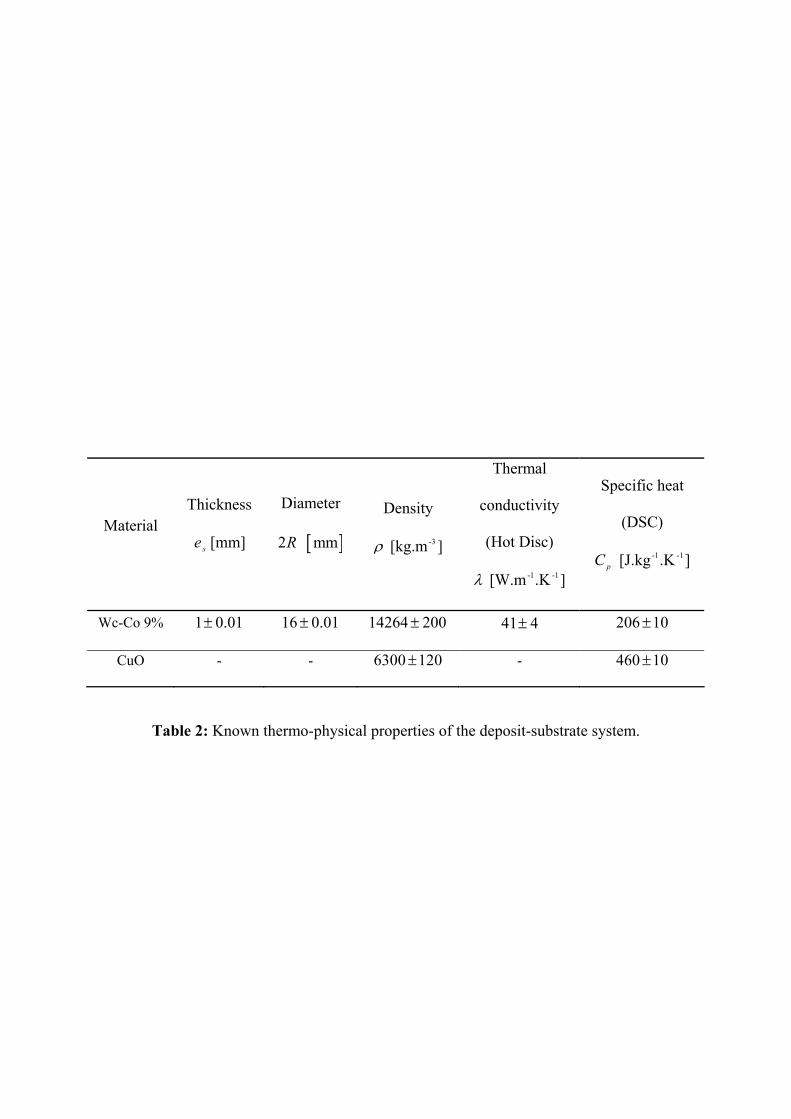
scale the measured gain to the real one. The known thermal parameters (see table 2) are used
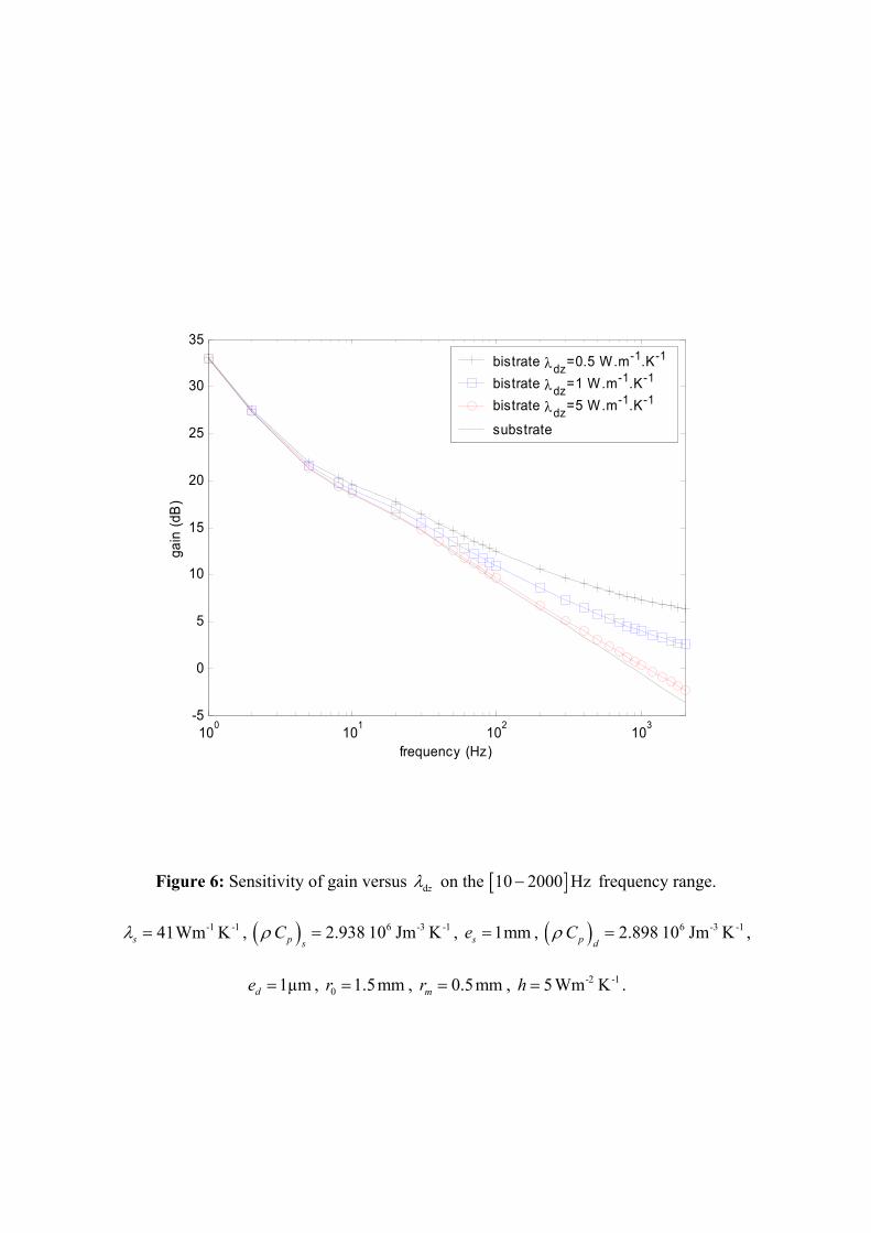
to plot the gain for different film conductivity values over the frequency interval 1-2000 Hz,
as represented in figure 6. The gain variation versus frequency for 200010 << f is small but
sufficient with regards to the measurement error in order to estimate the deposit thermal
conductivity.
Results
Deposit morphology The Wc-Co9% substrate is 16 mm diameter and 1 mm thickness. Uniformity of the deposition
surface roughness is reached from high pressure jet of calibrated Al2O3 particles (~3 µm
diameter). Surface is then cleaned by exposure to the ultrasounds. The surface morphology
has been measured using an optical interferometer device. Explored area is ( )80µm 60µm×
and the measurement has been repeated on three different zones of the surface in order to
verify the roughness uniformity. The 3D surface morphology is represented on figure 7. The
calculated average roughness is: nm 300=aR .
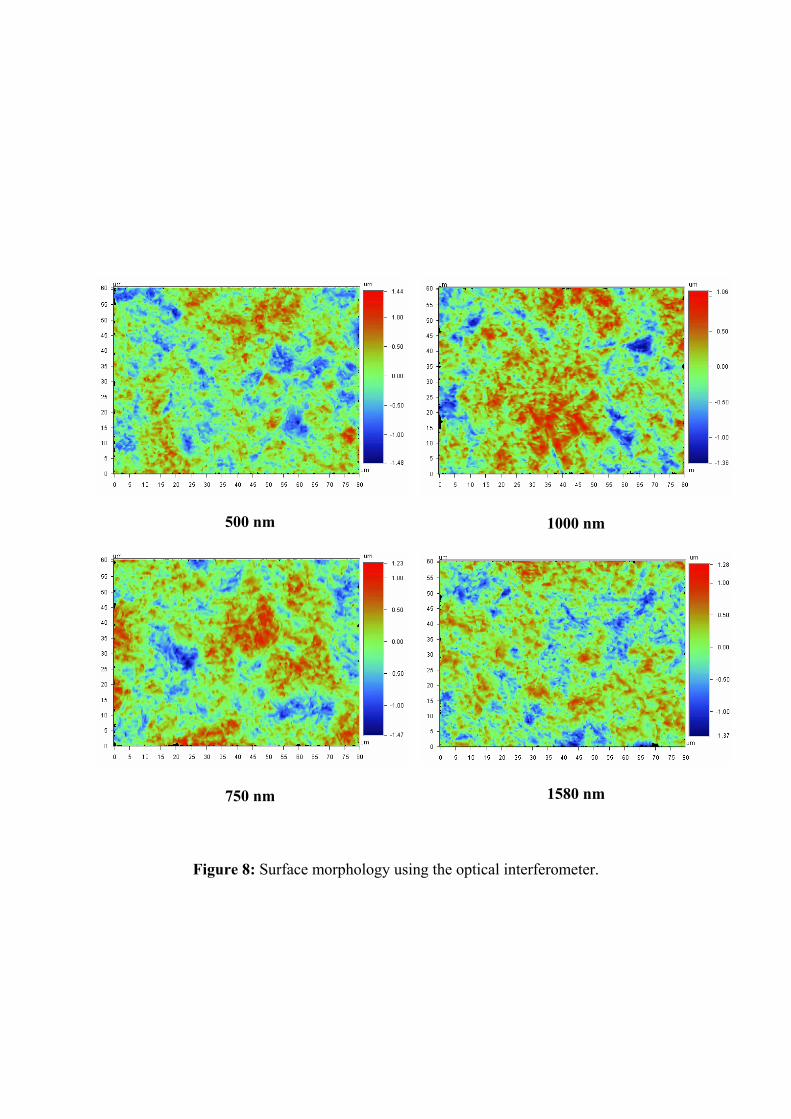
The CuO is deposited using the PVD technique. Process parameters are: RF power density 1.7
W/cm2, substrate temperature 25°C, deposition rate: 44.8 nm/min, total pressure: 0.5
Paoxygen, partial pressure 0.03 Pa (6%), crystallisation state: amorphous. Four samples have
been realized, considering different deposit thickness: 0.5 µm, 0.75 µm, 1 µm and 1.58 µm.
As previously, the 3D surface morphology has been measured for each sample and results are
presented in figure 8, roughness average values are reported in table 3. As one can see, the
roughness does not significantly vary whatever the deposit thickness. This result shows that
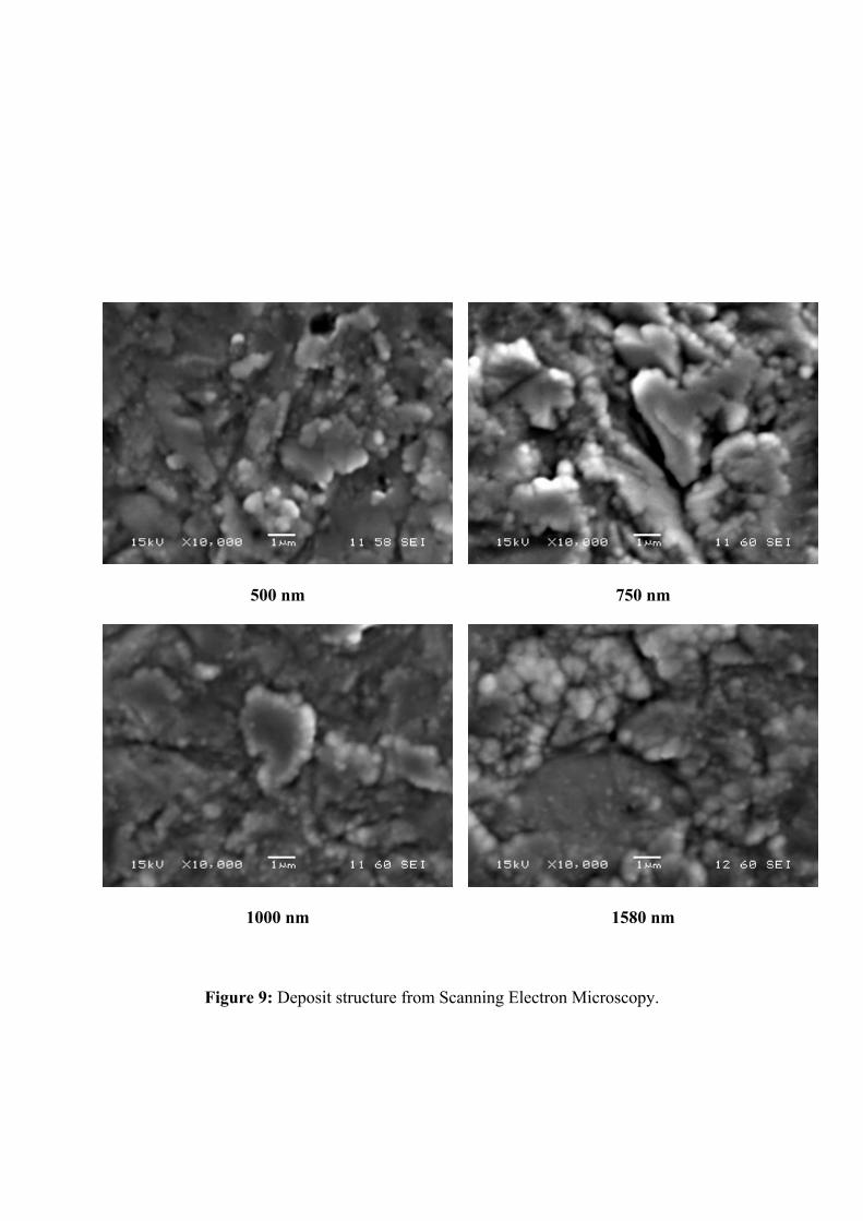
the deposit follows the substrate roughness. The film structure has been studied using
Scanning Electron Microscopy (SEM) apparatus. As represented on figure 9, the result is a
tapered columnar structure with the columns ending in domed tops as suggested in figure 1.
This is coherent with respect to the value of the temperature deposition: 0.3mT T < (where
mT is the CuO melting temperature). Whatever the deposit thickness, the average grain size is
approximately 1 µm and the deposit appears to be clearly anisotropic. Chemical composition
of each deposit is also measured using SEM and results are reported in table 4. It concerns an
average value in a 1µm thick layer from the deposit surface. It appears that the CuO
composition is homogeneous whatever the deposit thickness. Nevertheless, a small quantity
of Cobalt is observed even when the deposit thickness is greater than the explored depth. This
means that cobalt has diffused in the deposit during the deposition process. This result is
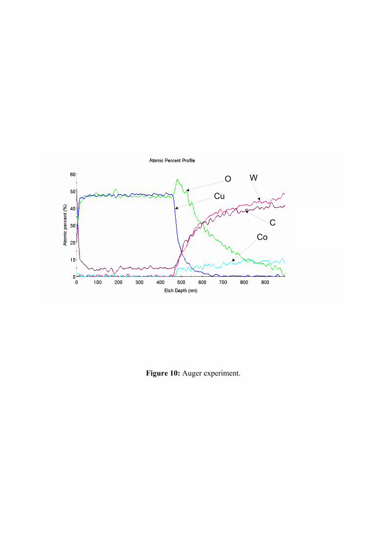
confirmed from the Auger experiment whose results are presented in figure 10.
Deposit conductivity The periodic photothermal experiments were carried out on four CuO film samples. The
explored frequency range is comprised between 10 Hz and 2 KHz, it was chosen according to
the sensitivity analysis presented in the previous section. The thermophysical properties of the
substrate were identified using the Hot Disk technique [13] for the thermal conductivity and
the Differential Scanning Calorimetric technique for the specific heat. The ( )p dCρ product
for the deposit was identified by the Differential Scanning Calorimetric for pC and
volumetric apparatus for ρ using the artificially obtained CuO crystals. These properties are
reported in table 2 with their standard deviations. The heat exchange with the ambient
characterized by h coefficient is: -1-2 K. W.m5 .
The deposit longitudinal thermal conductivity is identified by minimizing the quadratic gap
between the theorical and experimental values of the gain. The algorithm is a subspace trust
region method and is based on the interior-reflective Newton method described in [15] [14].
Each iteration involves the approximate solution of a large linear system using the method of
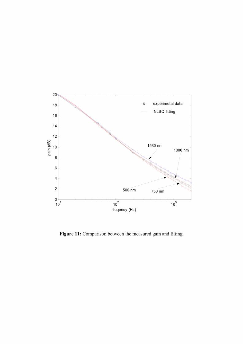
preconditioned conjugate gradients (PCG). Figure 11 represents the comparison of the
measured gain and the fitted one for each CuO film thickness.
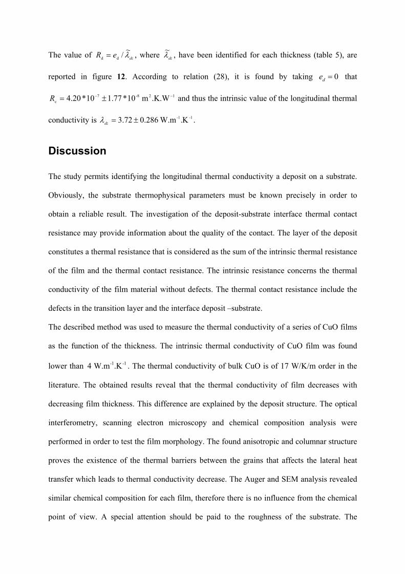
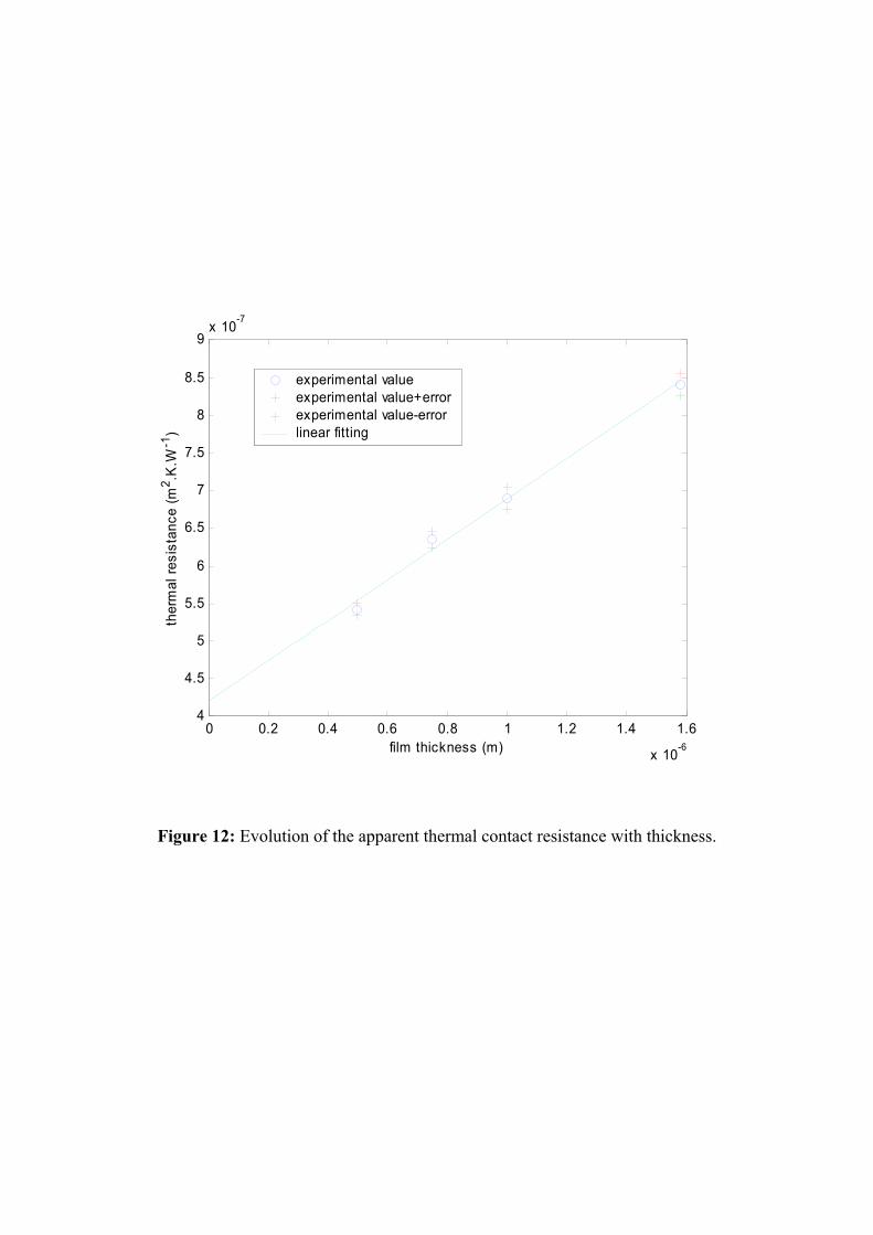
The value of dzeR λ~/dd = , where dzλ~ , have been identified for each thickness (table 5), are
reported in figure 12. According to relation (28), it is found by taking 0de = that
12-87c .K.Wm 10*1.7710*20.4 −− ±=R and thus the intrinsic value of the longitudinal thermal
conductivity is -1-1 K. W.m286.072.3 ±=dzλ .
Discussion
The study permits identifying the longitudinal thermal conductivity a deposit on a substrate.
Obviously, the substrate thermophysical parameters must be known precisely in order to
obtain a reliable result. The investigation of the deposit-substrate interface thermal contact
resistance may provide information about the quality of the contact. The layer of the deposit
constitutes a thermal resistance that is considered as the sum of the intrinsic thermal resistance
of the film and the thermal contact resistance. The intrinsic resistance concerns the thermal
conductivity of the film material without defects. The thermal contact resistance include the
defects in the transition layer and the interface deposit –substrate.
The described method was used to measure the thermal conductivity of a series of CuO films
as the function of the thickness. The intrinsic thermal conductivity of CuO film was found
lower than -1 -14 W.m .K . The thermal conductivity of bulk CuO is of 17 W/K/m order in the
literature. The obtained results reveal that the thermal conductivity of film decreases with
decreasing film thickness. This difference are explained by the deposit structure. The optical
interferometry, scanning electron microscopy and chemical composition analysis were
performed in order to test the film morphology. The found anisotropic and columnar structure
proves the existence of the thermal barriers between the grains that affects the lateral heat
transfer which leads to thermal conductivity decrease. The Auger and SEM analysis revealed
similar chemical composition for each film, therefore there is no influence from the chemical
point of view. A special attention should be paid to the roughness of the substrate. The
roughness does not change after deposition process, what signify that the coating follows
exactly the substrate form. In the thermal analysis, a plane surface of the film is considered. In
reality, at the scale of µm, this surface is constituted of peaks and valleys covered by the film
columns. The identified thermal conductivity of such deposit can be viewed as the average
between the longitudinal and the transversal one, especially that the experimental technique
leads to measurement on 1 mm diameter disk. The presented modeling of the heat transfer in
the studied system distinguishes two-directional conductivity. The identification of plane
conductivity will be extension of this work.
The morphology and chemical composition of thin film depend on the deposition process
parameters [11]. Certainly, the thermal conductivities of films realized in different condition
will be different. Moreover, the evolution of thermal conductivity according to thickness may
also differ between series realized in different condition.
Conclusion
The periodic technique for the thermal conductivity measurement was presented. It is based
on gain measurement from an infrared photothermal experiment. An optimum modulation
frequency range was defined. The experimental constraints limit it to 2 kHz. The study shows
similar low frequency behaviour for the uncoated substrate and the deposit-substrate system.
This behaviour permits to scale the measured gain to the real one in the thermal diffusion
process. The axis-symmetric model of heat transfer was used to fit the experimental data, and
identify the longitudinal thermal conductivity of the film, considering the exact knowledge of
the substrate parameters. The measurement on deposits with various thickness shows the
thickness dependence of the thermal conductivity of CuO films on tungsten carbide
substrates. It decreases linearly as the film thickness decrease from 1580 nm to 500 nm.
Considering the film as the thermal resistance has led determine the thermal contact resistance
between the deposit and the substrate and the longitudinal intrinsic thermal conductivity of
the film. As previously, the thermal resistance presents strong thickness dependence. In fact
thin film deposited by PVD or CVD on a substrate largely differs in its structure from a solid
material. A study concerning the films of the same thickness deposited at different
temperatures and so on with different morphologies will be complement to this work.
References
[1] Cahill D.G., Bullen A., Lee S.-M., Interface thermal conductance and the thermal conductivity
of multilayer thin films, High Temperatures-High Pressures, Vol. 32, pp. 134-142, 2000.
[2] Orain S., Scudeller Y., Brousse T., Thermal conductivity of ZrO2 thin films, International
Journal of Thermal Science, Vol. 39, pp. 537-543, 2000.
[3] Dilhaire S., Grauby S., Claeys W., Batsale J.-Ch., Thermal parameters identification of
micrometric layers of microelectronic devices by thermoreflectance microscopy,
Microelectronics Journal, Vol. 35, pp. 811-816, 2004.
[4] Faugeroux O ., Caractérisation thermophysique de revêtements de protection thermomécanique
par méthode photothermique impulsionelle, PhD thesis, Université de Perpignan, 2001.
[5] Gagliano O., Etude multi échelles des transferts de chaleur dans les revêtements métalliques
réfractaires, PhD thesis, Université Aix-Marseille III, 2002.
[6] Bodnar J.-L., Lannoy B., Durville L., Radiométrie photothermique sous excitation aléatoire par
analyses corrélatoire et paramétrique, Congrès de la Société Française de Thermiciens, pp. 637-
642, 1996.
[7] Bhusari D.M., Teng C.W., Chen K.H., Wei S.L., Chen L.C, Traveling wave method for
measurement of thermal conductivity of thin films", Rev. Sci. Instrum. 68 (11), pp. 4180-4183,
1997.
[8] Langer G., Hartmann J., Reichling M., Thermal conductivity of thin metallic films measured by
photothermal profile analysis, Rev. Sci. Instrum. 68 (3), pp. 1510-1513, 1997.
[9] Chen G., Particularities of heat conduction in nanostructures, Journal of Nanoparticle Research,
Vol. 2, pp. 199-204, 2000.
[10] Ju Y.S., Goodson K.E., Phonon scattering in silicon films, Appl. Phys. Lett. Vol. 74, pp. 3005-
3007, 1999.
[11] Sheppard K. G., Nakahara S., The microstructure and morphology of thin films, Processing of
Advanced Materials, Vol. 1, pp. 27-39, 1991.
[12] Incropera F.P., DeWitt D.P., Introduction to Heat Transfer, John Wiley and Sons, 1996.
[13] Gustavsson, M., Karawacki, E., Gustafsson, S.E., Thermal conductivity, thermal diffusivity and
specific heat of thin samples from transient measurements with hot disk sensors. Rev. Sci. Instr.,
Vol. 65, pp. 3856-3859, 1994.
[14] Coleman, T.F. and Y. Li, "An Interior, Trust Region Approach for Nonlinear Minimization
Subject to Bounds," SIAM Journal on Optimization, Vol. 6, pp. 418-445, 1996.
[15] Coleman, T.F. and Y. Li, "On the Convergence of Reflective Newton Methods for Large-Scale
Nonlinear Minimization Subject to Bounds," Mathematical Programming, Vol. 67, Number 2,
pp. 189-224, 1994.

r
z
deposit
substrate
0
r0
R
es
ed
ϕ <T0>
λdz
λdr
Figure 1: Deposit thermal characterisation using the front face experiment. A transient heat
flux density ϕ is applied on the deposit surface (over the disc of radius 0r ) and one measures
the average temperature 0T on the heated area.
function generator
sample
HgCdTe detector
elliptical mirror
focal pointsof the elliptic mirror
mirroir
laser diode
semitransparentmirrorphotodiode
lock-in amplifier
oscilloscope
pre-amplifier
convex lens
5%
95%
Figure 2: Schematic view of the experimental setup.
0 5 10 150
10
20
30
40
50
60
70
80
90
100
wavelength(µm)
valu
e (%
)
rhodium reflectivityspectral response of HgCdTe
Figure 3: Spectral response of the infrared detector and the mirror reflectivity in function of
the wavelength.
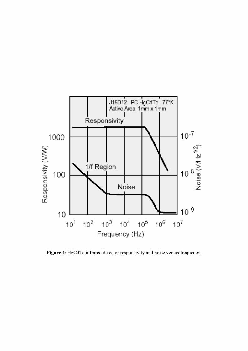
Figure 4: HgCdTe infrared detector responsivity and noise versus frequency.
ϕ0
<θ0>
Zd Zs
1/h 1/h
Rc
ϕ0
<θ0>
Zs
1/h 1/h
Rd
f << ad/ed2
Figure 5: Corresponding electrical analogy of the heat transfer model in the deposit-substrate
system.
100 101 102 103-5
0
5
10
15
20
25
30
35
frequency (Hz)
gain
(dB
)
bistrate λdz=0.5 W.m-1.K-1
bistrate λdz=1 W.m-1.K-1
bistrate λdz=5 W.m-1.K-1
substrate
Figure 6: Sensitivity of gain versus dzλ on the [ ]10 2000 Hz− frequency range.
-1 -141Wm Ksλ = , ( ) 6 -3 -12.938 10 Jm Kp sCρ = , 1mmse = , ( ) 6 -3 -12.898 10 Jm Kp d
Cρ = ,
1µmde = , 0 1.5mmr = , 0.5mmmr = , -2 -15Wm Kh = .
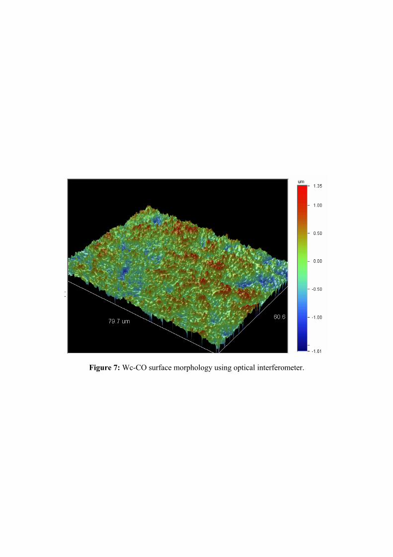
Figure 7: Wc-CO surface morphology using optical interferometer.
500 nm 1000 nm
750 nm 1580 nm
Figure 8: Surface morphology using the optical interferometer.
500 nm 750 nm
1000 nm 1580 nm
Figure 9: Deposit structure from Scanning Electron Microscopy.
O W
Cu
C
Co
Figure 10: Auger experiment.
101 102 1030
2
4
6
8
10
12
14
16
18
20
freqency (Hz)
gain
(dB
)
1580 nm 1000 nm
500 nm 750 nm
experimetal data o
NLSQ fitting
Figure 11: Comparison between the measured gain and fitting.
0 0.2 0.4 0.6 0.8 1 1.2 1.4 1.6
x 10-6
4
4.5
5
5.5
6
6.5
7
7.5
8
8.5
9x 10⁻⁷
film thickness (m)
ther
mal
resi
stan
ce (m
2 .K.W
-1)
experimental valueexperimental value+errorexperimental value-errorlinear fitting
Figure 12: Evolution of the apparent thermal contact resistance with thickness.
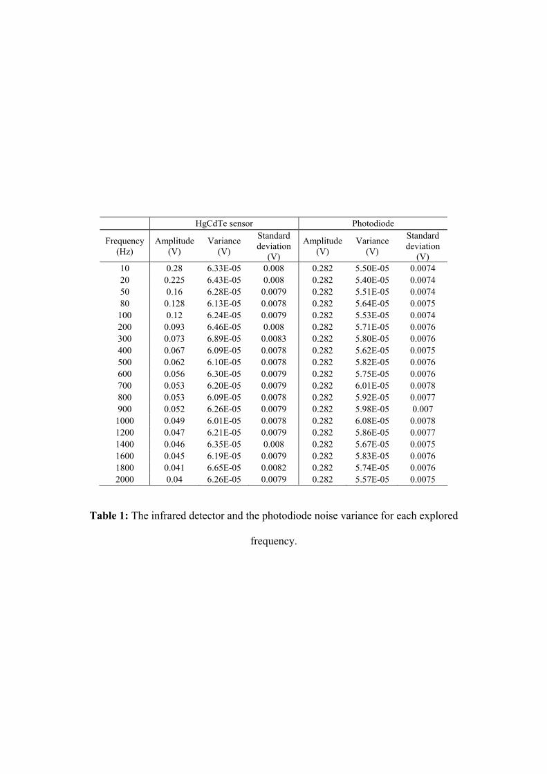
HgCdTe sensor Photodiode
Frequency (Hz)
Amplitude (V)
Variance (V)
Standard deviation
(V)
Amplitude (V)
Variance (V)
Standard deviation
(V) 10 0.28 6.33E-05 0.008 0.282 5.50E-05 0.0074 20 0.225 6.43E-05 0.008 0.282 5.40E-05 0.0074 50 0.16 6.28E-05 0.0079 0.282 5.51E-05 0.0074 80 0.128 6.13E-05 0.0078 0.282 5.64E-05 0.0075
100 0.12 6.24E-05 0.0079 0.282 5.53E-05 0.0074 200 0.093 6.46E-05 0.008 0.282 5.71E-05 0.0076 300 0.073 6.89E-05 0.0083 0.282 5.80E-05 0.0076 400 0.067 6.09E-05 0.0078 0.282 5.62E-05 0.0075 500 0.062 6.10E-05 0.0078 0.282 5.82E-05 0.0076 600 0.056 6.30E-05 0.0079 0.282 5.75E-05 0.0076 700 0.053 6.20E-05 0.0079 0.282 6.01E-05 0.0078 800 0.053 6.09E-05 0.0078 0.282 5.92E-05 0.0077 900 0.052 6.26E-05 0.0079 0.282 5.98E-05 0.007 1000 0.049 6.01E-05 0.0078 0.282 6.08E-05 0.0078 1200 0.047 6.21E-05 0.0079 0.282 5.86E-05 0.0077 1400 0.046 6.35E-05 0.008 0.282 5.67E-05 0.0075 1600 0.045 6.19E-05 0.0079 0.282 5.83E-05 0.0076 1800 0.041 6.65E-05 0.0082 0.282 5.74E-05 0.0076 2000 0.04 6.26E-05 0.0079 0.282 5.57E-05 0.0075
Table 1: The infrared detector and the photodiode noise variance for each explored
frequency.
Material Thickness
[mm] se
Diameter
[ ]2 mmR
Density
][kg.m -3ρ
Thermal
conductivity
(Hot Disc)
].K[W.m -1-1λ
Specific heat
(DSC)
].K[J.kg -1-1pC
Wc-Co 9% 1 0.01± 16 0.01± 14264 200± 41 4± 206 10±
CuO - - 6300 120± - 460 10±
Table 2: Known thermo-physical properties of the deposit-substrate system.
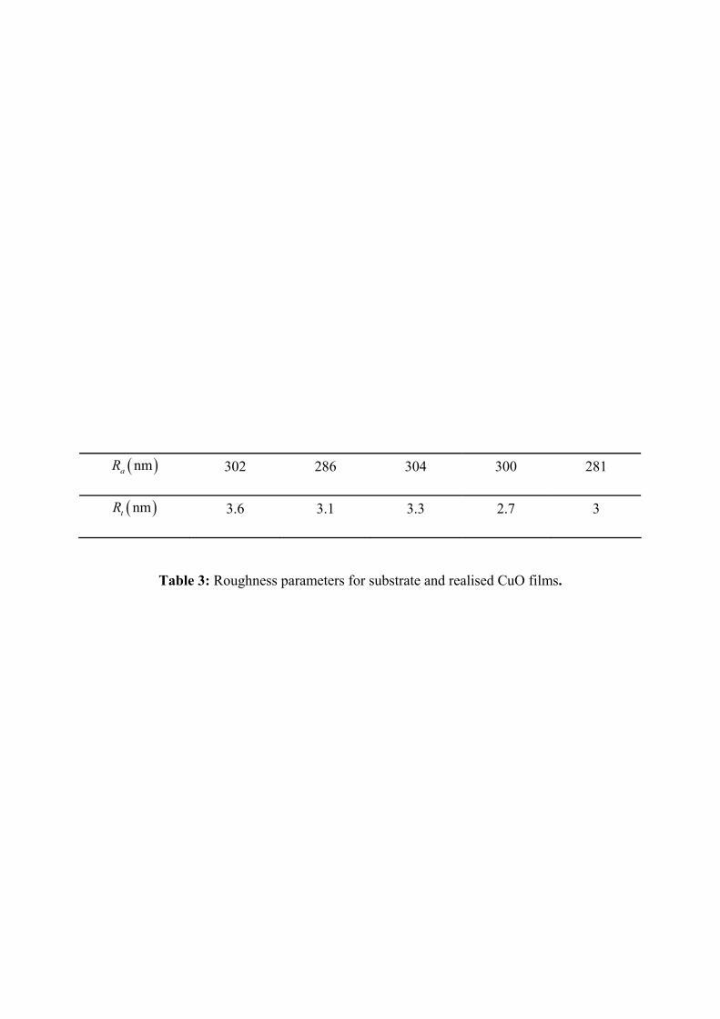
( )nmaR 302 286 304 300 281
( )nmtR 3.6 3.1 3.3 2.7 3
Table 3: Roughness parameters for substrate and realised CuO films.
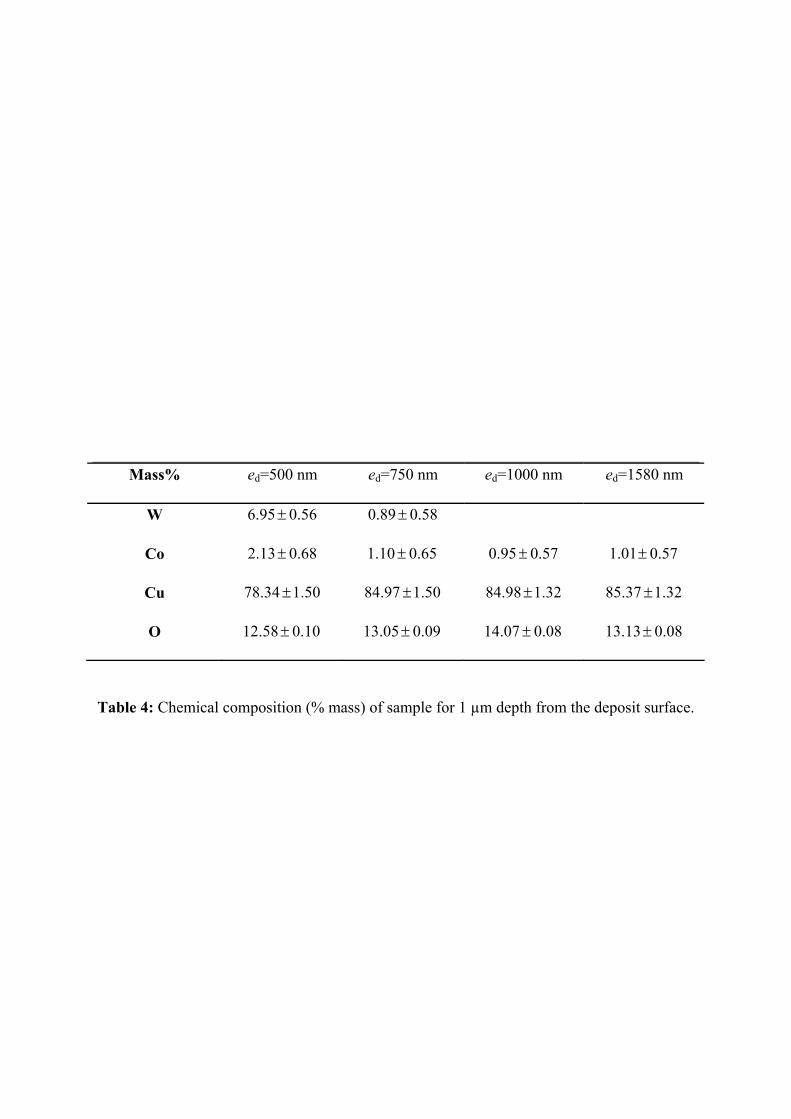
Mass% ed=500 nm ed=750 nm ed=1000 nm ed=1580 nm
W 6.95 0.56± 0.89 0.58±
Co 2.13 0.68± 1.10 0.65± 0.95 0.57± 1.01 0.57±
Cu 78.34 1.50± 84.97 1.50± 84.98 1.32± 85.37 1.32±
O 12.58 0.10± 13.05 0.09± 14.07 0.08± 13.13 0.08±
Table 4: Chemical composition (% mass) of sample for 1 µm depth from the deposit surface.
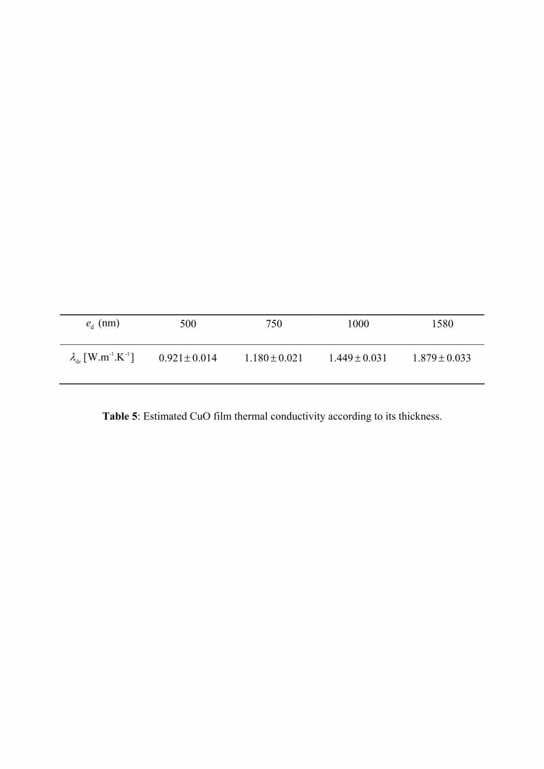
de (nm) 500 750 1000 1580
]K.W.m[ -1-1dzλ 0.921 0.014± 1.180 0.021± 1.449 0.031± 1.879 0.033±
Table 5: Estimated CuO film thermal conductivity according to its thickness.


![Improved conductivity and capacitance of interdigital ...mai.group.whut.edu.cn/chs/lw/2016/201702/P... · polymer fabrication techniques with pyrolysis or thermal degradation [21–27]](https://img.pdfslide.fr/doc/110x75/5ff7dcadced30417a4176688/improved-conductivity-and-capacitance-of-interdigital-maigroupwhuteducnchslw2016201702p.jpg)